- 易迪拓培训,专注于微波、射频、天线设计工程师的培养
The causes of these errors in CST MWS
录入:edatop.com 点击:
Hi, everyone!
Here I have some problems of a PCB simulation. The job is to test the radiation of a clock circult of a FPGA chip.
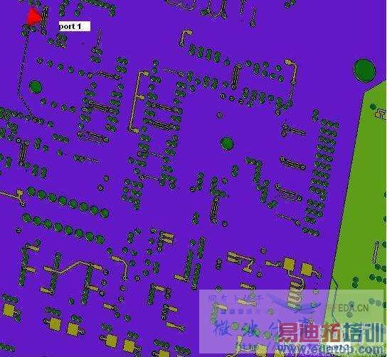
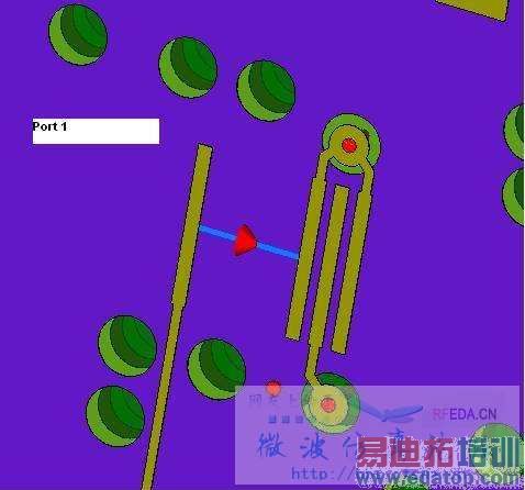
1: I imported the model to CST MWS and defined 2 discrete ports at the start and the end of that circult respectively.
2: I adjusted the mesh properties with the consideration of reducing the simulation time, and now the mesh number is in an acceptable quantity.
3: The solver is FDTD and then some problems happened.
I will attach a graph to explain the problem more clearly. Hope some guys could help me out with these problems or some tips are good enough:)!
Modified your post to adjust the picture size.
hefang
Modified your post to adjust the picture size.
hefang
Here I have some problems of a PCB simulation. The job is to test the radiation of a clock circult of a FPGA chip.
1: I imported the model to CST MWS and defined 2 discrete ports at the start and the end of that circult respectively.
2: I adjusted the mesh properties with the consideration of reducing the simulation time, and now the mesh number is in an acceptable quantity.
3: The solver is FDTD and then some problems happened.
I will attach a graph to explain the problem more clearly. Hope some guys could help me out with these problems or some tips are good enough:)!
Modified your post to adjust the picture size.
hefang
So, what are the problems?
PS: CST MWS transient solver uses FIT but not FDTD.
what·s the meaning you were trying to express? what is your problem?
Im really really sorry. I forgot to mention the problems that day.
The problem is: After I launched the simulation, there happened a problem that: the discrete port 1 and 2 are in the perfect conducted metal plane (Im sorry I couldnt remember the exact description as now the CST is occupied by others, thus I can't run it again and attach the graph.)
I found it...Thanks for your patience, guys:) 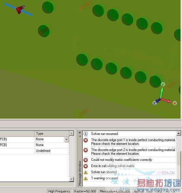
Modified your post to adjust the picture size.
hefang
Any chance to upload your model file?
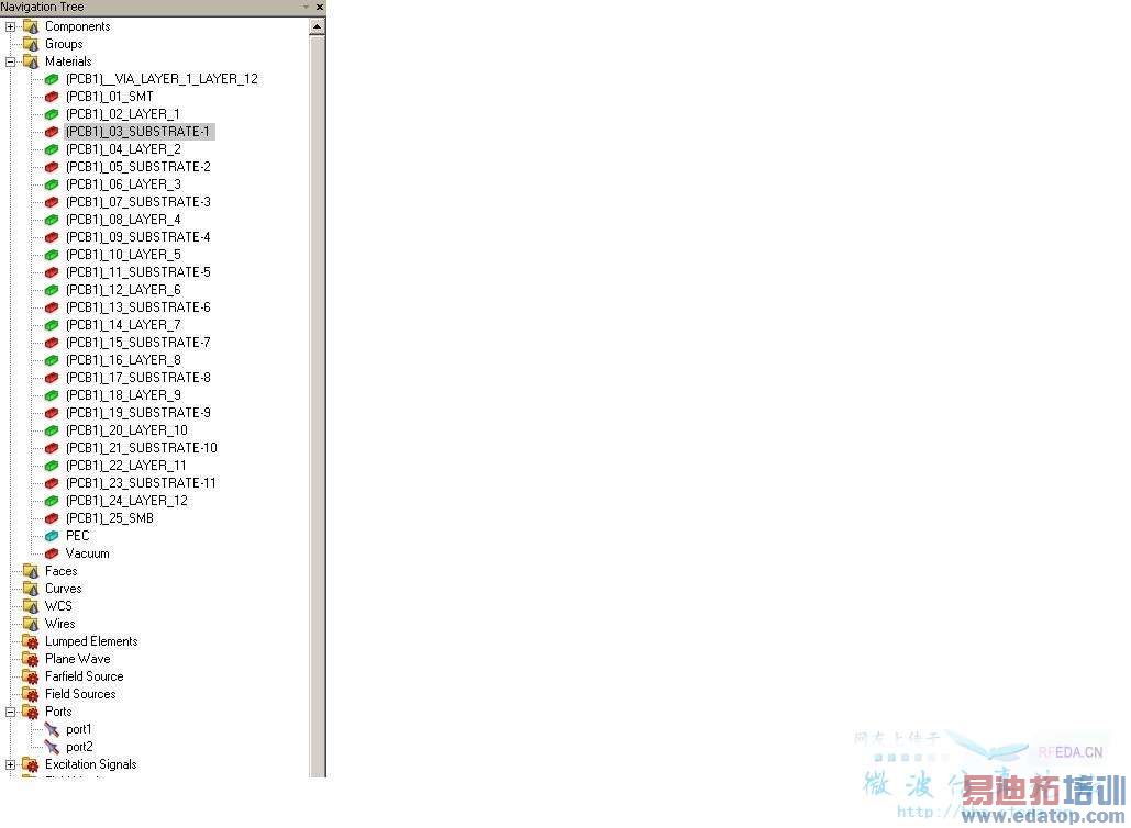
1. What are the purple and green solids' (substrates) material properties?
2. What's the background material in your model?
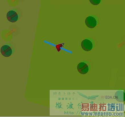
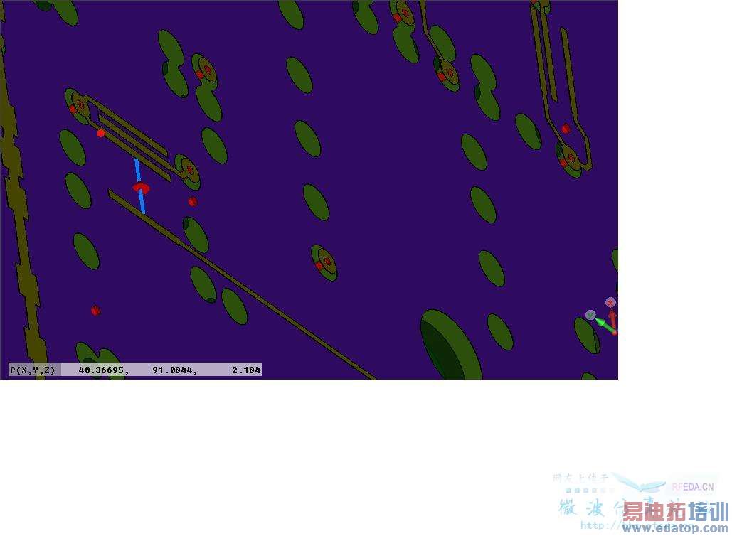
mesh view, you will find that the center of the port have been changed.
I'd like to upload my model but unfortunately, it is seriously against the company rules, and I can't even take this file back home. That's why I can only ask you guys while im working and in English.
Anyway, I'll try to explain the model: This PCB is made of 12 layers, between each two, there is a substrate layer
The material of 12 layers is LOSSY METAL, with 5.8e+007 S/m electric conductivity, Mue =1
The material of the substrates is NORMAL; with Epsilon (relative dielectric constant )=4.3, Mue =1
Hefang, you've asked me about the meaning of the purple and green solids, well, these represent the different layers. The purple one is the second layer, and I believe that both the port 1 and port 2 locate on the layer 1 (The metal micro strip in graph 2). As for the green one, it's hard to tell which layer it is because the similar colors of the adjacent layers that my colleagues used.
Depend on the snapshots without physically "see" the model, it's hard for me to locate the root cause.
What's the total thickness of the PCB, as well as the thickness of the copper and the substrate (the seperation of layers)?
Or, as haihun suggested, active the mesh view and check the discrete port location. What is the global mesh properties? I noticed that you reduced the mesh numbers. Then it's a potential risk in low mesh density that the actual discrete port location in meshviewis NOT the same in modelling view. If the ports touch any of the coppers, then the error message is reasonable.
申明:网友回复良莠不齐,仅供参考。如需专业解答,请学习易迪拓培训专家讲授的CST视频培训教程。
上一篇:求一个RFID天线的模型
下一篇:lumped port 箭头方向有讲究吗?