- 易迪拓培训,专注于微波、射频、天线设计工程师的培养
请大家来看下,Creat Netlist 时报的错!已解决!
录入:edatop.com 点击:
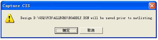
上面的图是我运行Creat Netlist 第一次弹出来的对话框。
然后出现下面的框,出错误了。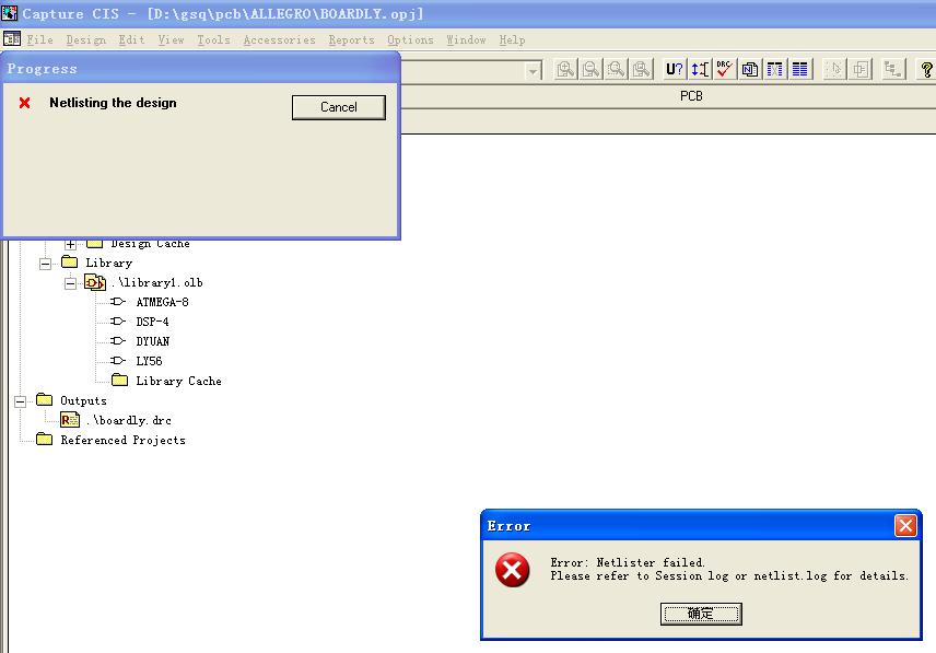
我到netlist.log里面,发现只有下面一段话。
{ Using PSTWRITER 10.5.0 p001Sep-27-2006 at 13:58:01 }
#1 Error [ALG0039] No components to package in design.
#2 Aborting Netlisting... Please correct the above errors and retry.
我不知道是什么原因,是不是封装库路径不对?希望大家帮忙
谢谢!
我的msn:gsq_by@msn.com 刚开始学ALLEGRO,但在其他方面可以相互学习。
Error [ALG0039] No components to package in design
Either no components are placed on the schematic or all placed components are to be excluded from the netlist. For example, if all components are assigned the PSpiceOnly property, there would be no netlist. To eliminate this error, you must use components besides those with just the PSpiceOnly property when creating an Allegro netlist.
看不懂。
首先check 原理图,没有一个错误。然后在create Netlist。
谢谢你的关注!
Design Rules Check 已经通过。
如下:
Checking Pins and Pin Connections
--------------------------------------------------
Checking Schematic: mcuall.SchDoc
--------------------------------------------------
Checking Electrical Rules
Checking for Unconnected Nets
Checking for Invalid References
Checking for Duplicate References
Check Bus width mismatch
--------------------------------------------------
Checking Schematic: BOARDLY
--------------------------------------------------
Checking Electrical Rules
Checking for Unconnected Nets
Checking for Invalid References
Checking for Duplicate References
Check Bus width mismatch
原理图里某些元件没有指定footprint
footprint 都添加了。大小写也都改过了。还是没解决
不知道封装的路径对不对?
1 Error [ALG0039] No components to package in design.
这句话是什么意思呢?元气件不能封装? 是不是我封装的路径要设置下?在CAPTURE 还是ALLEGRO中设置呢?
PROTEL里导过来的,里面隐藏了一些东西,没有封装。
我选中EDIT才看的到,肉眼根本看不出来,是隐型的,NND!
以后吸取个教训。
谢谢:zxpchx/layoutmaster的帮助。
我也出现同样的问题,哎
Cadence Allegro 培训套装,视频教学,直观易学
上一篇:skill encypt
下一篇:急需 allegro \软件