- 易迪拓培训,专注于微波、射频、天线设计工程师的培养
怎么控制约束net上的pin pair
录入:edatop.com 点击:
Hi all,
In my FPGA-DDR2 design, on the net of A8, there is a pullup resistor. Please refer the attached pix for the layout on my board.
The path I need to control prop delay is from FPGA to DDR2. But in Allegro, pin pairs on this net is R-FPGA or R-DDR2, as following from information on this net:
< NET >
Net Name: DDR2_A8
Member of Bus: DDR2_ADDR
Pin count: 3
Via count: 2
Total etch length: 1582.389 MIL
Total manhattan length: 1652.899 MIL
Percent manhattan: 95.73%
Pin Type SigNoise Model Location
--- ---- -------------- --------
U2.T29 BI CDSDefaultIO (5652.756 3039.055)
P2.93 IN CDSDefaultInput (6383.000 2921.728)
RP8.1 UNSPEC DEFAULT_RESISTOR_PACK_4_47OHM (6899.800 2633.200)
No connections remaining
Properties attached to net
LOGICAL_PATH = @\penguin-1\.schematic1(sch_1):ddr2_a8
FSP_NET = DDR2_A<0>
BUS_NAME = DDR2_ADDR
Electrical Constraints assigned to net
prop delay: from AD to AR min=1600.000 MIL max=2200 ns
relative prop delay: global group DDR2_ADDR_CTRL_CLK from AD to AR delta=0.000 MIL tol=280.000 MIL
max parallelism: 300 MIL length at 6 MIL separation
max parallelism: 600 MIL length at 7 MIL separation
max parallelism: 1000 MIL length at 8 MIL separation
max parallelism: 2000 MIL length at 10 MIL separation
FSP_NET: DDR2_A<0>
Constraint information:
(Dly) RP8.1 to U2.T29 max= 2200ns actual= 1447.605 MIL (0.235986ns)
(6899.800,2633.200) pin RP8.1,UNSPEC,TOP/TOP
767.468 MIL (0.114477ns) cline TOP
(6258.000,2898.109) via TOP/BOTTOM
652.3 MIL (0.117235ns) cline SIG4
(5672.440,3058.740) via TOP/BOTTOM
27.838 MIL (0.00427453ns) cline TOP
(5652.756,3039.055) pin U2.T29,BI,TOP/TOP
(Dly) RP8.1 to P2.93 min= 1600 MIL actual= 902.251 MIL
(6899.800,2633.200) pin RP8.1,UNSPEC,TOP/TOP
767.468 MIL cline TOP
(6258.000,2898.109) via TOP/BOTTOM
134.783 MIL cline BOTTOM
(6383.000,2921.728) pin P2.93,IN,BOTTOM/BOTTOM
(RDly) RP8.1 to U2.T29 min= 2056.43 MIL max= 2616.43 MIL actual= 1447.605 MIL
target= (DDR2_CKE0) RP5.2 to U2.U31
(6899.800,2633.200) pin RP8.1,UNSPEC,TOP/TOP
767.468 MIL cline TOP
(6258.000,2898.109) via TOP/BOTTOM
652.3 MIL cline SIG4
(5672.440,3058.740) via TOP/BOTTOM
27.838 MIL cline TOP
(5652.756,3039.055) pin U2.T29,BI,TOP/TOP
Member of Groups:
MATCH_GROUP : DDR2_ADDR_CTRL_CLK
BUS : DDR2_ADDR
PHYSICAL & SPACING NETCLASS: 8MIL
Can anybody give me some advice to make control on the path from FPGA to DDR2?
Thanks!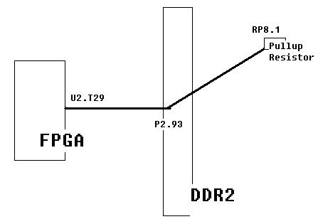
如果你的net接线是FPGA-->R.1--R.2-->DDR2这种模式你可以建立Xnet形式,就会产生FPGA到DDR2的pin pair了,
如果你的net接线是FPGA-->DDR2-->R.1--R.2(上拉是接电源,下拉是接地)这种模式,你可以在constraint manager里面直接产生FPGA到DDR2的pin pair
Cadence Allegro 培训套装,视频教学,直观易学
上一篇:vista怎么不能安装15.7啊?求高手赐教
下一篇:allegro使用交换管脚功能后如何反标到orcad的原理图