ST STW82100B 1850-2400 MHz下变换解决方案
The STMicroelectronics STW82100B is an integrated down converter providing 8 dB of gain, 10.5 dB NF, and a very high input linearity by means of its passive mixer.
Embedding two wide band auto calibrating VCOs and an integer-N synthesizer, the STW82100B is suitable for both Rx and Tx requirements for Cellular infrastructure equipment.
The integrated RF balun and internal matching permit direct 50 ohm single-ended interface to RF port. The IF output is suitable for driving 200-ohm impedance filters.By embedding a DAC with dual current output to drive an external PIN diode attenuator, the STW82100B replaces several costly discrete components and offers a significant footprint reduction.
The STW82100B device is designed with STMicroelectronics advanced 0.35 μm SiGe process. Its performance is specified over a -40℃ to +85℃ temperature range.
STW82100B主要特性:
■ High linearity:
– IIP3: +25.5 dBm
– 2FRF-2FLO spurious rejection: 77 dBc
■ Noise figure:
– NF: 10.5 dB
■ Conversion gain
– CG: 8dB
■ RF range: 1850 MHz to 2400 MHz
■ Wide IF amplifier frequency range: 70 MHz to 400 MHz
■ Integrated RF balun with internal matching
■ Dual differential integrated VCOs with automatic center frequency calibration:
– LOA: 1650 to 1950 MHz
– LOB: 2050 to 2370 MHz
■ Embedded integer-N synthesizer – Dual modulus programmable prescaler (16/17 or 19/20)
– Programmable reference frequency divider (10 bits)
– Adjustable charge pump current
– Digital lock detector
– Excellent integrated phase noise
– Fast lock time: 150 μs
■ Integrated DAC with dual current output
■ Supply: 3.3 V and 5 V analog,3.3 V Digital
■ Dual digital bus interface: SPI and I2C bus (fast mode) with 3 bit programmable address(1101A2A1A0)
■ Process: 0.35 μm BICMOS SiGe
■ Operating temperature range -40 to +85oC
■ 44-lead exposed pad VFQFPN package7x7x1.0 mm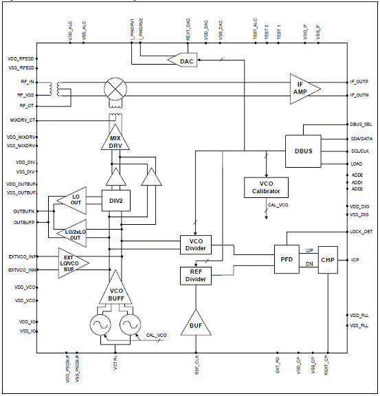
图1。STW82100B方框图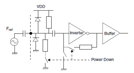
图2。STW82100B参考频率输入缓冲器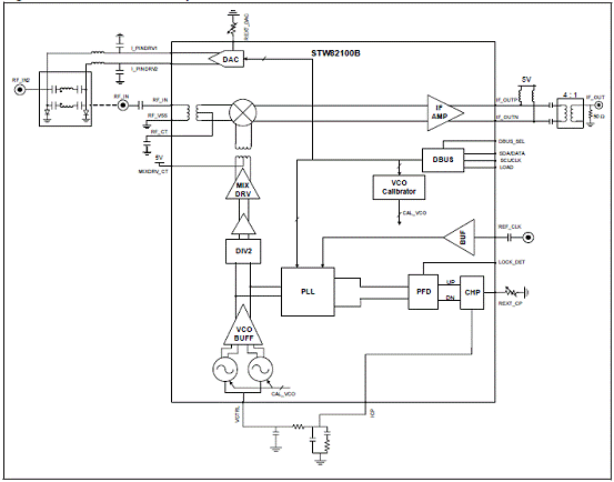
图3。STW82100B标准模式工作框图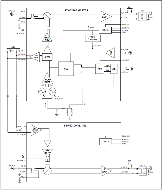
图4。STW82100B采用相同LO频率的多模式工作框图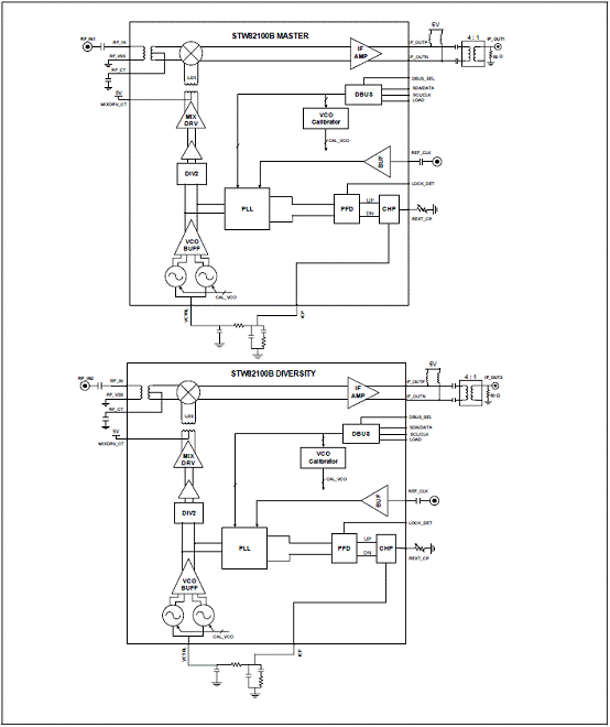
图5。STW82100B采用不同LO频率的多模式工作框图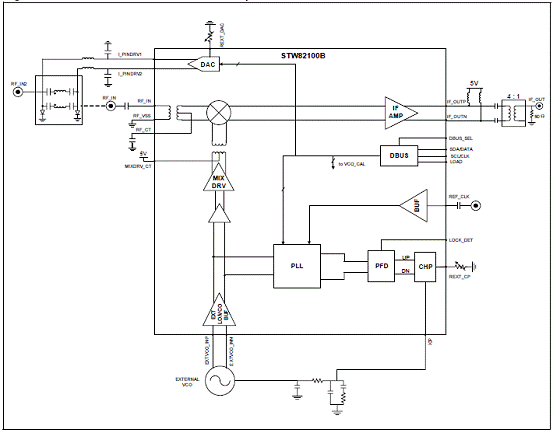
图6。STW82100B采用外接VCO的标准模式工作框图
图7。STW82100B采用相同LO频率的外接VCO多模式工作框图
图8。STW82100B典型应用电路图
应用电路材料清单:
详情请见:
http://www.st.com/internet/com/TECHNICAL_RESOURCES/TECHNICAL_LITERATURE/DATASHEET/CD00295270.pdf
