HFSS 3D Layout
录入:edatop.com 点击:
-
Introduction
-
Start HFSS 3D Layout
-
3D Layout for PCB
-
問題與討論(Q&A)
6.1 How to set HPC for 3D Layout?
6.2 How to set roughness in 3D Layout?
6.3 Does via plating work in 3D Layout?
6.4 How to add embedded component to 3D Layout?
6.5 How to do if you encounter initial mesh failure issue?
6.6 How to eliminate the non-passivity issue in 3D Layout?
How to eliminate the surface mesh failure in 3D Layout?
6.7 How to use Q3D solver to solve DC point in 3D Layout?
6.8 How to set "non-model" property to a object in 3D Layout?
6.9 How to remove\preserve non-functional pads in 3D Layout?
6.10 What benefit would 3D Layout with multi-solution frequency get?
6.11 What is the difference between gap\wave\circuit port in 3D Layout?
6.12 Can SIwave launch 3D Layout with RLC components automatically?
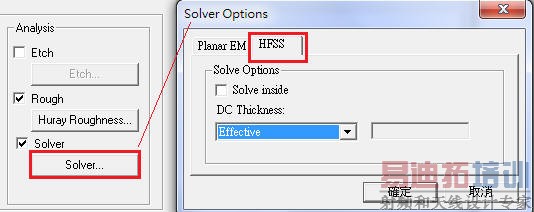
6.13 How to set "solve inside" and DC Thickness manually in 3D Layout?
6.14 Does it work to run wave, gap and circuit ports together in a project?
6.15 How to disable port auto-creation when SIwave export to 3D Layout?
6.16 Can 3D Layout export far-field emission test report (EMI) and W-element model?
6.17 Does 3D Layout support wave port de-embed to extend the length of transmission line?
6.18 Does 3D Layout support two neighbor metal layers (touched without dielectric inserted)?
6.19 If several HFSS setup solutions exist in 3D Layout (PlanarEM), how to assign what you want?
-
Reference
-
Introduction
1.1 What is "HFSS 3D Layout"?
"HFSS 3D Layout" is a new feature from HFSS 2014. It uses an innovated meshing technology (Phi-mesh) for layer structures, and is much more faster for initial mesh (x30~60 speed-up). You can treat "HFSS 3D Layout" as a solution that is HFSS 3D solver + SIwave GUI \ PlanarEM GUI.
1.2 Why is "HFSS 3D Layout"?
Much more faster for initial mesh.
Easy to use (create ports easily).
Specially good for PCB SI\PI\EMI analysis (including 2-layer PCB) and complex LC component extraction of chip level.
-
Start HFSS 3D Layout
2.1 Run it through SIwave Platform
Identify power\ground plane
Create ports in SIwave (that is exactly "circuit port")
Check the nets to analyze
Run HFSS 3D Layout from the menu of SIwave
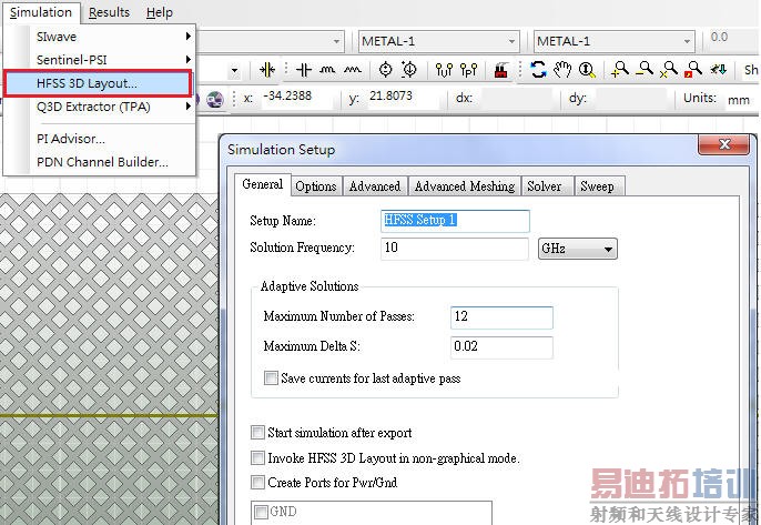
For SIwave's ports, the same ones will be created automatically in HFSS 3D Layout.
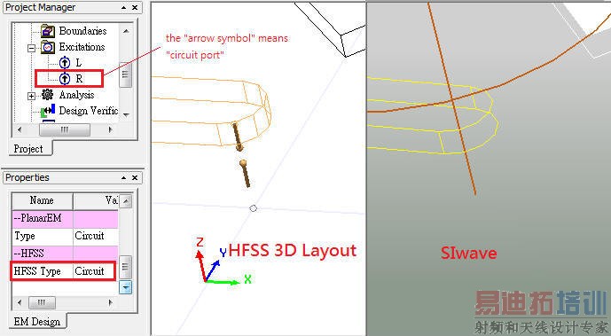
SIwave的circuit port與HFSS 3D Layout的circuit port還是有些不同;前者是SPICE type,後者是Field type (有較大的寄生電感效應)
HFSS 3D Layout generates Gap port \ Gap(coax) ports for the terminals of wire bonds and solder balls.
"Gap port" is like the "lump port" you knew in HFSS before.
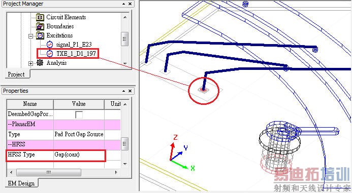
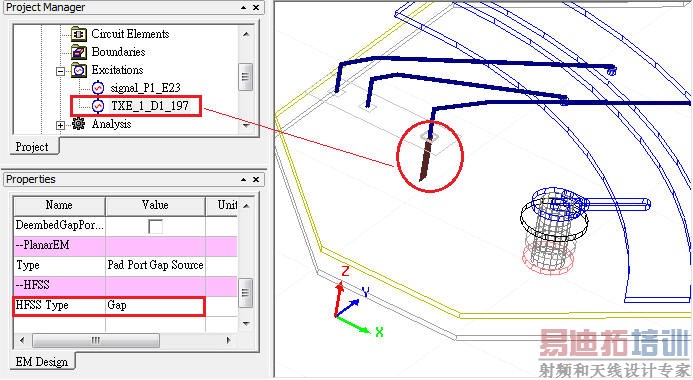
Avoid setting a gap port with long length to minimize the parasitic inductance. (even it cab be de-embed)
2.2 Run it through PlanarEM Platform
Create a PlananEM Design
Import .anf
Add HFSS solution setup
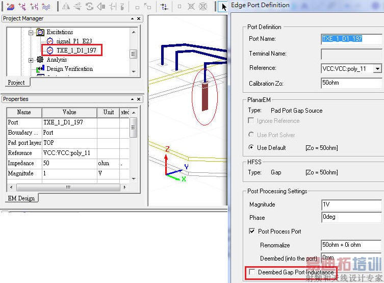
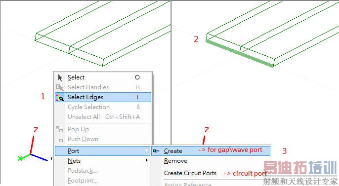
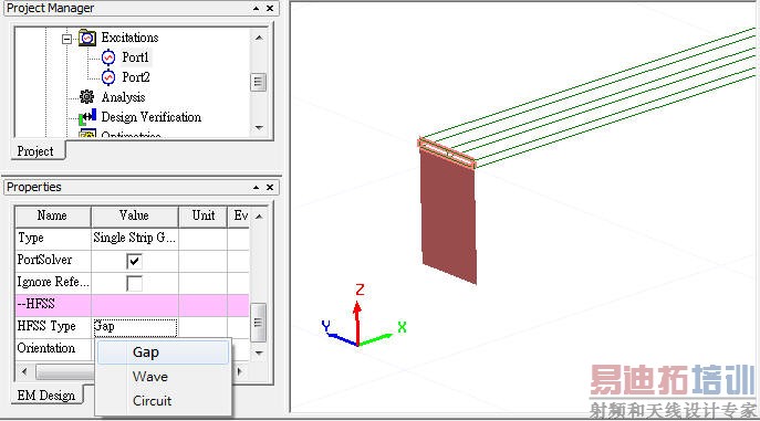
You can select the edge of an object, then create a port (gap\wave\circuit port).
-
問題與討論(Q&A)
6.1 How to set HPC for 3D Layout?
Ans:Set it from Designer \ Electronics Desktop, not from SIwave GUI.

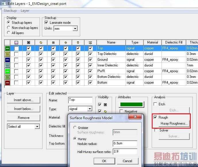
6.2 How to set roughness in 3D Layout?
Ans:[Layout] \ [Layers]

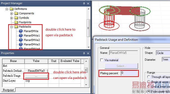
6.3 Does via plating work in 3D Layout?
Ans:For R17.x, the answer is yes. It takes more time to solve if via plating is set, but the S-parameter with plating is almost the same as the one without plating. In fact, this is an expected result, via plating effect is more pronounced at low frequency, and how much it affects that depends on the through hole radius and wall thickness of via.
By the way, it is easy to use both of SIwave and HFSS 3D layout to confirm\correlate the S-parameter results are almost the same for a via with plating or not. If you would like to see the difference (RLDC) of via plating effect, SIwave DC analysis is the best solution, and you can find about 0.2 mohm difference between full fill and 20% plating for a via with 0.15mm inner radius.
Accessing to via stack-up from [Layout] \ [ViaStyle] or double click as below to open a padstack usage and definition window.
6.4 How to add embedded component to 3D Layout?
Ans:
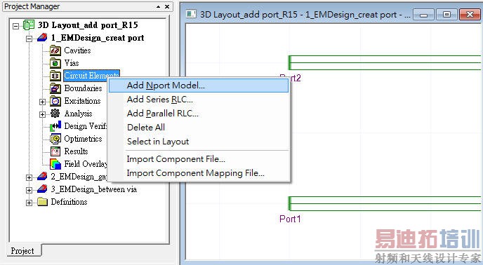
如果沒辦法add embedded component (RLC or S-parameter),請先把圖面以正視圖擺正
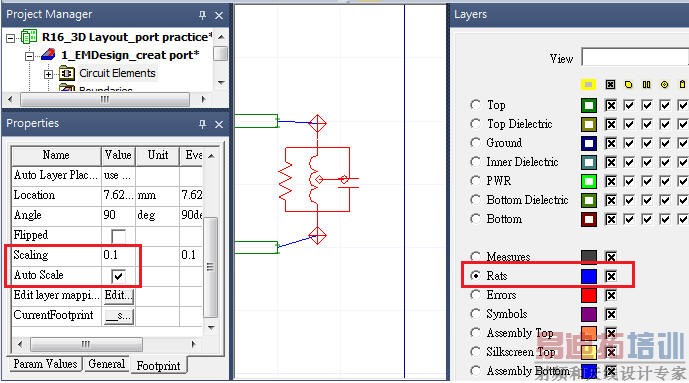
R16如果看不到已經畫好的鼠線,請確認[Rats]有被打開,並試著以放大縮小重新刷新畫面
6.5 How to do if you encounter initial mesh failure issue?
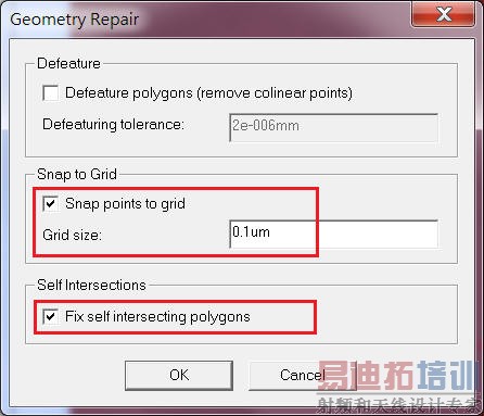
Ans:First, try to do geometry repair
[Draw] \ [Defeature and Repair] with R17.x
[Draw] \ [Geometry Healing] with R18.x
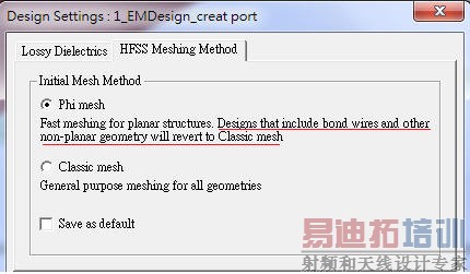
The second way, change to use "class mesh" that is always better for layer structure.
R15 PlanarEM, [EM Design] \ [Design Settings]
R16 Electronic Desktop, [HFSS 3D Layout] \ [Design Settings]
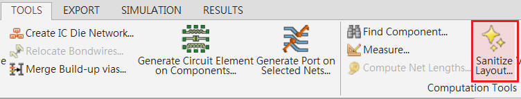
The third way, back to SIwave(ALink) to do [Tools] \ [Sanitize Layout]
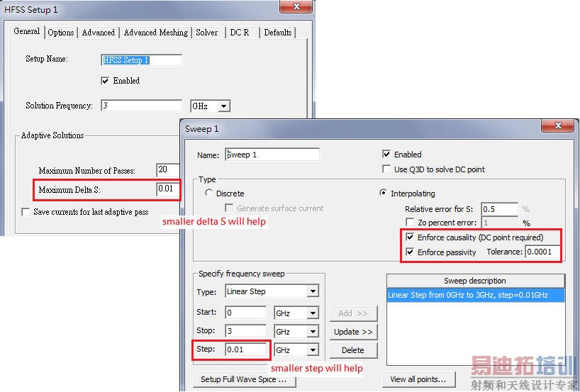
6.6 How to eliminate the non-passivity issue in 3D Layout?
Ans:
Set smaller "Max. Delta S" for refine mesh, for example 0.02 -> 0.01 -> 0.001 with min. converged passes=2, and check [enforce passivity] term.
6.6.2 How to eliminate the surface mesh failure in 3D Layout?
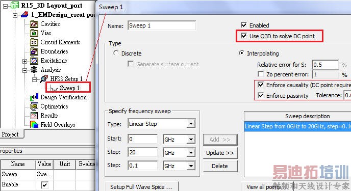
6.7 How to use Q3D solver to solve DC point in 3D Layout?
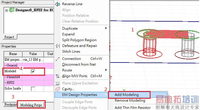
6.8 How to set "non-model" property to a object in 3D Layout?
Ans:Select the object, then [Draw] \ [EM Design Properties] \ [Add Modeling]
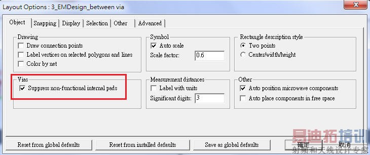
6.9 How to remove\preserve non-functional pads in 3D Layout?
Ans:[Layout] \ [Setting] \ [Object Tab]
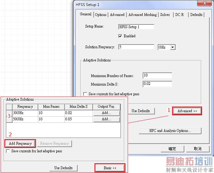
6.10 What benefit would 3D Layout with multi-solution frequency get?
Ans:傳統HFSS只有一個求解頻點(solution frequency, adaptive frequency),HFSS除了基於這頻點決定initial mesh的品質(for example, zero order uses 1/10 lambda refinement),也基於這頻點做refine mesh。對於waveguide filter或EBG的應用,在某些頻段範圍能量是完全不會傳遞的,若solution frequency正好設在這範圍內,會導致HFSS無法很好的以判斷error percent做refine mesh。像AN010 SIwave\9.4的例子,HFSS的solution frequency就不能設40G以上,否則S-parameter的結果就會有問題,此時如果有兩個solution frequency就可確保refine mesh的品質(準確)。
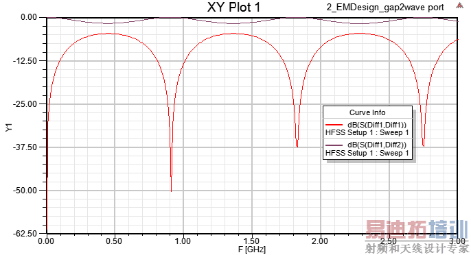
6.11 What is the difference between gap\wave\circuit port in 3D Layout?
Ans:
Circuit port are very easy to use as they can be added anywhere. This would really speeds up especially for the designs with large port count, that we find in SI and PI application. They should primarily be used between two terminals that are electrically close to each other without any geometry intersection of the current path. Since circuit ports carry current, they have associated inductance and unlike the de-embedded lump port technology built on an analytic model for rectangular conductors, the arbitrary nature of the circuit ports means there is no general analytic model for their partial inductance that can be de-embedded.
-- circuit port越短越好,否則會引入無法de-embed的寄生電感效應
-- 雖然允許在任意兩點之間下circuit port,但如果有導體擋在電流路徑間,那就不能讓circuit port跨過 (as crossing plane layer)
6.12 Can SIwave launch 3D Layout with RLC components automatically?
Ans:Yes.
6.13 How to set "solve inside" and DC Thickness manually in 3D Layout?
Ans:A finite conductivity boundary is used for conducting layers by default.
6.14 Does it work to run wave, gap and circuit ports together in a project?
Ans:Yes, but the mixed usage of wave and gap port sometimes seems to cause non-passivity issue, be careful.
6.15 How to disable port auto-creation when SIwave export to 3D Layout?
Ans:SIwave 2015, [Edit] \ HFSS [3D Layout] ports, select the row and check "deactivate" for the ports of wire-bonds or solder-balls
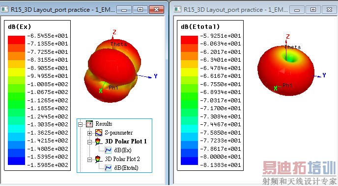
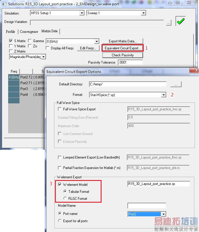
6.16 Can 3D Layout export far-field emission test report (EMI) and W-element model?
Ans:
6.16.1 3D Layout can export far-field \ 3D Polar Plot, but not far-field "emission test report"
6.16.2 3D Layout can export W-element model
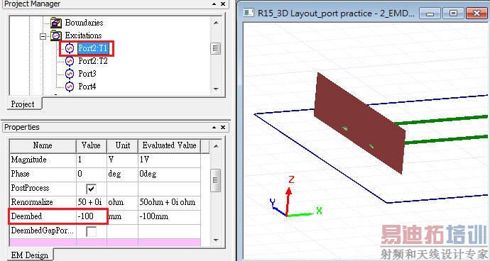
6.17 Does 3D Layout support wave port de-embed to extend the length of transmission line?
Ans:Yes, R15 supports it well, but something tricky here.
-- Just the [Deembed] parameter in the first terminal of the wave port can be set by user, and the others will be synchronized automatically
-- Although de-embed is post-process, you still need to press [F10] to refresh the result again
-- Wave port de-embed just affects S-parameter, not far-field result
6.18 Does 3D Layout support two neighbor metal layers (touched without dielectric inserted)?
Ans:SIwave can't support two neighbor metal layers touched without dielectric inserted, but 3D Layout can.
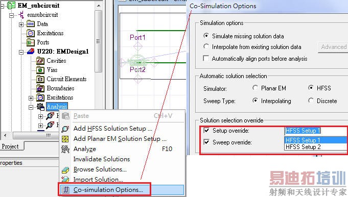
6.19 If several HFSS setup solutions exist in 3D Layout (PlanarEM), how to assign what you want?
Ans:
本文来源:网际星空(oldfriend.url.tw);EDATOP整理(www.edatop.com)
HFSS 学习培训课程套装,专家讲解,视频教学,帮助您全面系统地学习掌握HFSS
上一篇:从HFSS12到HFSS2017,Ansys HFSS 各版本的主要新增功能
下一篇:HFSS各版的主要新增功能