- 易迪拓培训,专注于微波、射频、天线设计工程师的培养
DEK delivers Solar Solutions for the Thin-Film Generation
录入:edatop.com 点击:
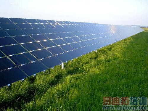
DEK Solar has revealed that its PV1200 photovoltaic metallization platform is not only being deployed around the world to meet the challenges of silicon wafers but also, to meet the commercial challenges of thin-film substrates. Using its proven experience in the solar sector, DEK is driving the production of thin-film PV cells towards mass market adoption through a range of cost and productivity benefits.
The emergence of new types of solar cells produced using thin-film technology presents solar manufacturers with a number of advantages including cost benefits against increasingly expensive silicon wafers. For example, thin-film technology enables solar cells to be constructed on flexible substrates, opening up many new opportunities to embed solar power generation into diverse commercial applications. Working closely with influential producers, DEK has developed a range of metallization solutions for thin-film substrates. Processes include precision deposition of silver epoxy compounds for metallization, as well as the application of other active and interconnect layers, using printing techniques similar to those already proven in bulk silicon solar cell production.
"As the production of solar cells increases globally, producers need better and faster production technology, backed by shorter lead-times and customer support capable of supporting ongoing productivity," explains DEK’s Alternative Energy Business Development Manager, Darren Brown. "Here at DEK Solar, we’ve already established world-class production values for companies building photovoltaic cells on silicon wafers and we’re delighted that we can now deliver the same opportunities to thin-film cell producers. Combined with leading-edge production technology, our global support infrastructure provides even the most progressive companies with the back-up they need to maximise throughput and yield. What’s more, I’m confident that our commitment to partnering with our customers will continue to optimise the production of thin-film solar cells for mass-market adoption into the future."
Delivering 1200 cells-per-hour throughput, six-sigma process rating, 12.5 micron resolution and advanced handling capabilities, DEK’s PV1200 solar metallization line leverages the company’s 40 years of experience developing mass imaging platform products. In addition to well-established technical advantages, the DEK Solar metallization line also benefits from a global network of support resources, spares hubs, applications expertise and field service technicians. DEK Solar customers also benefit from in-house screens capabilities, developing the precision technologies critical to the metallization process in a state-of-the-art Class 10,000 clean room manufacturing facility.
For more information about how DEK Solar could help you meet your thin-film challenge, please visit www.deksolar.com.
About DEK Solar
DEK is a global provider of next-generation technologies and process support to solar cell manufacturers with solutions that include modular metallization platforms, precision screens and materials applications used in back side field coating, current-collector pattern and termination deposition for photovoltaic substrate production. For more information, visit DEK Solar at www.deksolar.com.