- 易迪拓培训,专注于微波、射频、天线设计工程师的培养
[ADS] Voltage Multiplier and its input impedance in ADS ?
录入:edatop.com 点击:
Respected Members,
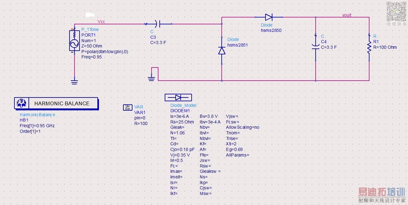
I have designed a voltage multiplier/Doubler at 950 MHz (0.95 GHz)(Figure below). I am having some trouble in terms of its functionality and design. If you could clarify the following;
1. Is my circuit design appropriate/correct (i.e. simulators, lumped components, values, and rest parameters)?
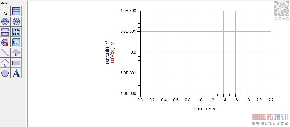
2. Why Im not getting any input voltage Vcc and its multiplied output voltage Vout?
3. Any help available or a sample design tutorial in ADS for a voltage multiplier?
4. Finally, I would like to find out what is the input impedance of the circuit at different input power and frequency so that I can proceed with the design of an impedance matching network which will be placed in between a 50 ohm antenna and the voltage doubler. May I know how can I do that in ADS?
Could anyone please help?
Thanks.
I have designed a voltage multiplier/Doubler at 950 MHz (0.95 GHz)(Figure below). I am having some trouble in terms of its functionality and design. If you could clarify the following;
1. Is my circuit design appropriate/correct (i.e. simulators, lumped components, values, and rest parameters)?
2. Why Im not getting any input voltage Vcc and its multiplied output voltage Vout?
3. Any help available or a sample design tutorial in ADS for a voltage multiplier?
4. Finally, I would like to find out what is the input impedance of the circuit at different input power and frequency so that I can proceed with the design of an impedance matching network which will be placed in between a 50 ohm antenna and the voltage doubler. May I know how can I do that in ADS?
Could anyone please help?
Thanks.
From first look, your source works with 0.95 Hz! not GHz. As I understood, you want to rectify your voltage and have some DC-voltage? You can easily plot impedances vs. frequency with for example s-paramters. Just have a look in the manual.
1 and 2) are you sure about the 0.95 GHz working frequency and 3.3 Farad capacitors?
Note that your Source is working at 0.95 Hz while your HB simulation is running at 0.95 GHz
3) There is no ADS Design Guide for Voltage Doublers (that I know of)
4) If you want to know the input impedance perform Large Signal S-Parameter Simulation (LSSP) and plot the reflection coefficient (S11) of the circuit in a Smith Chart
Best regards and good luck
@johnjoe: @viper_iv
sorry about the values mistake..My source is 0.95 GHz and C=3.3 nF with R=100 Kohm...Figure updated...And yes I need to rectifiy my circuit to get a DC voltage..
So any helot abt Voltage doubler frm this updated figure given below...
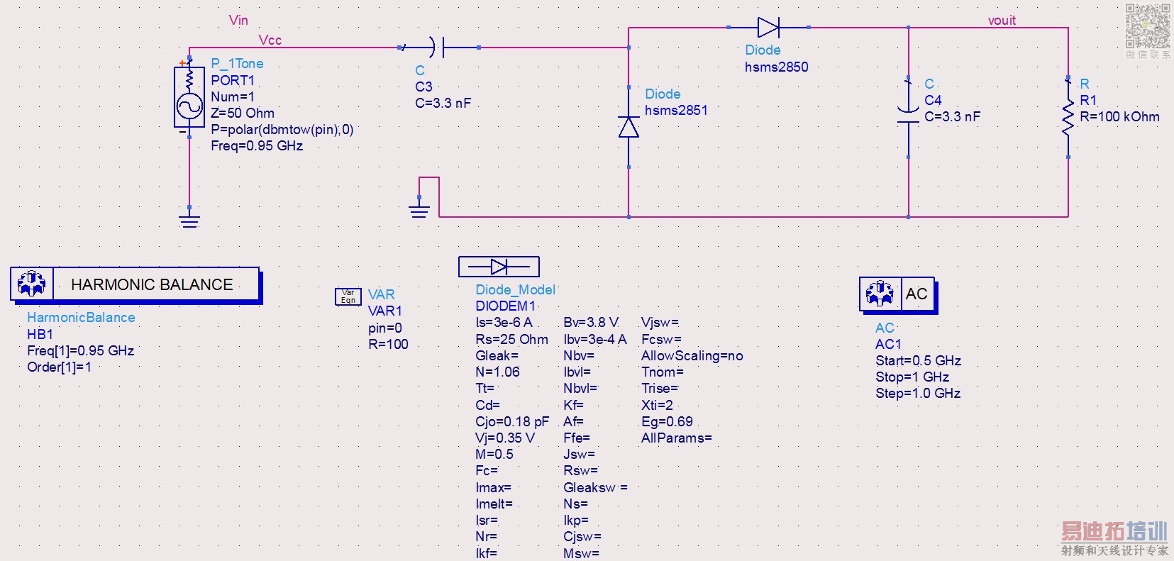
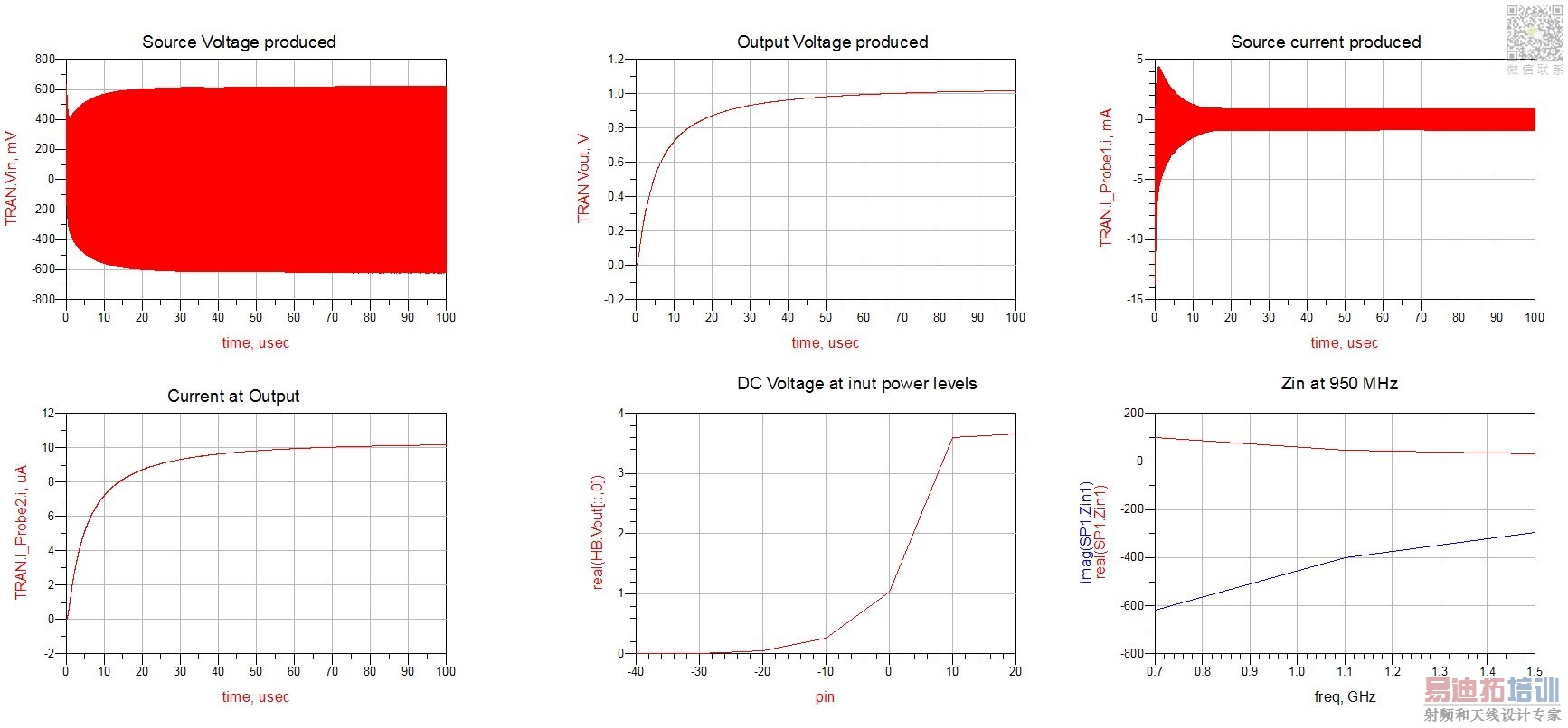
The configuration you have is working for me (I get a 1.08 V signal at the output)
However, you should only use the Harmonic Balance and Large-Signal S parameters solvers for this case (not AC)
Im still not getting any input or output voltage..
@viper_iv: Could u kindly share ur ADS file that produced the results at ur end.
Here you go...
Is the file provided an ADS file..Its not supported..
@johnjoe: I re-did the simulation and I'm getting output and input wave forms but the output is not Doubled...Images attached...Any reason u knw of? Anyone ...
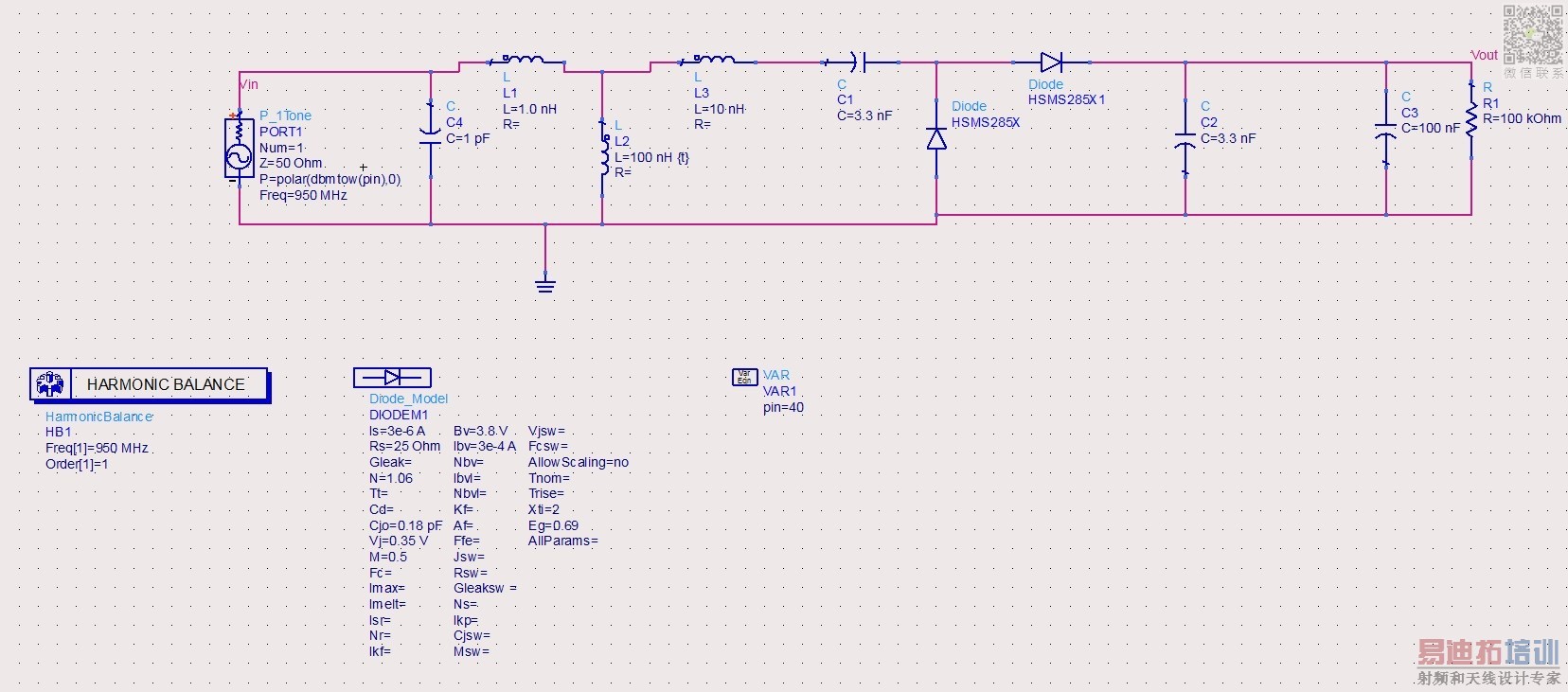
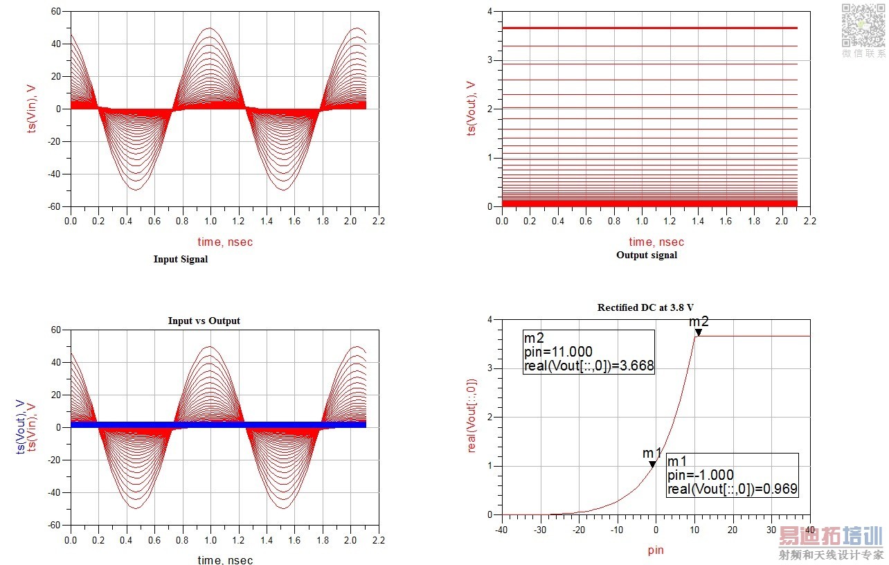
First, it's ads 2011 schematic file, you have to import the file into the library directory of an existing project. For first try, remove the coils and the 1pF cap. I used the ideal diodes with your model specification, maybe try this.
I added my sim and schematic pics and the complete ads 2011 project.
Thankyou for the project, Ill continue with the structure first without coils and thn making the doubler.Thnx again
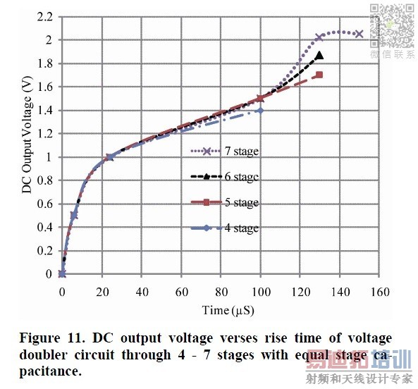
@johnjoe: One more query. I want to know how many stages would produce the max DC voltage. I have seen a paper where its plotted as below.
Is there any function in ADS to use a single voltage doubler , make its [n] stages and see the DC results?
@johnjoe:
I added additional 7-stages of Voltage doubler to your design in-order to get more output DC Voltage but its not improving. Should I attach the file?
You can upload if you want.
Ok. Ill message u.
Please post everything in the forum, not as private message.
First mistake: Your source frequency is 0.95 GHz, your HB-frequency is 0.95 Hz, change the value of swp_freq.
Second mistake: The circuit is not correct . I uploaded a corrected version. Steady state solution shows an multiplied voltage but from transient analysis it's obvious that it takes some time, maybe you can optimize it.
Ok.I'll post everything here.
Thankyou for pointing out a major mistake. I'll update the circuit and report back soon.
@johnjoe: So As seen in the figures below, I get 1V at one stage multiplier. But when I move to two stage voltage doubler the voltage reduces to 14 mV with optimized C values.
File attached. Kindly assist.

Did you checked my uploaded schematic? It is a multi-stage voltage multiplier based on your Greichnacher circuit.
You can refer to this thesis for some support http://ria.ua.pt/handle/10773/8717
But I believe you won't get that much increase in efficiency/output voltage after 3 stages
@johnjoe: Which uploaded file? Can u kindly re-post the multistage file.
@viper_iv: Thnx for the link, but atleast I should get near to 5V for three stages...As pr theory
申明:网友回复良莠不齐,仅供参考。如需专业帮助,请学习易迪拓培训专家讲授的ADS视频培训课程。
上一篇:S11 matching circuit stimualtion with ADS
下一篇:NXP_LDMOS library Error in ADS
ADS培训课程推荐详情>>
 国内最全面、最专业的Agilent ADS培训课程,可以帮助您从零开始,全面系统学习ADS设计应用【More..】
- Agilent ADS教学培训课程套装
- 两周学会ADS2011、ADS2013视频教程
- ADS2012、ADS2013射频电路设计详解
- ADS高低阻抗线微带滤波器设计培训教程
- ADS混频器仿真分析实例视频培训课程
- ADS Momentum电磁仿真设计视频课程
- ADS射频电路与通信系统设计高级培训
- ADS Layout和电磁仿真设计培训视频
- ADS Workspace and Simulators Training Course
- ADS Circuit Simulation Training Course
- ADS Layout and EM Simulation Training Course
- Agilent ADS 内部原版培训教材合集