- 易迪拓培训,专注于微波、射频、天线设计工程师的培养
Need help for bias circuit 2 stage broadband LNA using ATF34143 in ads
录入:edatop.com 点击:
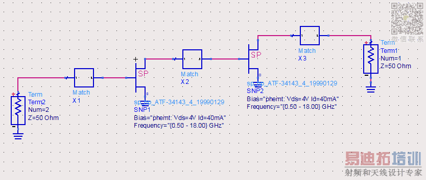
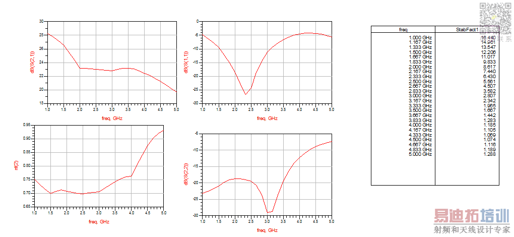
i have done small signal analysis for 2 stage amplifier using ATF34143 for 4V,40 mA for Vgs=-0.41 but i am new in this so i need help for gate bias and drain bias
i did already but i get harmonic distortion and low power added efficiency.
i want to know what should be Vgg if Vgs is found -0.41 V. does Rs required or inductor is enough in gate bias.
i have posted my results of small signal analysis and design without bias circuit
i did already but i get harmonic distortion and low power added efficiency.
i want to know what should be Vgg if Vgs is found -0.41 V. does Rs required or inductor is enough in gate bias.
i have posted my results of small signal analysis and design without bias circuit
ATF34143 is an LNA (Low Noise Amplifier), and by definition any LNA should work in Class-A.
So, good PAE (Power Added Efficiency) is not the main target of performances of this transistor.
For best performances follow the Avago application notes 1190 and 1191.
it was helpful but can you tell me, with this result can i design amplifier and if yes then how should i bias to achieve 4V 40 mA Q-point.. what should be my next step
Do i need to provide parallel tuned L C circuit for drain ? what should be value of Rg ?
申明:网友回复良莠不齐,仅供参考。如需专业帮助,请学习易迪拓培训专家讲授的ADS视频培训课程。
上一篇:Does anyone here knows where I can download the S2P file of a FET ADS
下一篇:I am trying to import a spice file netlist from Murata into ADS; not working.
ADS培训课程推荐详情>>
 国内最全面、最专业的Agilent ADS培训课程,可以帮助您从零开始,全面系统学习ADS设计应用【More..】
- Agilent ADS教学培训课程套装
- 两周学会ADS2011、ADS2013视频教程
- ADS2012、ADS2013射频电路设计详解
- ADS高低阻抗线微带滤波器设计培训教程
- ADS混频器仿真分析实例视频培训课程
- ADS Momentum电磁仿真设计视频课程
- ADS射频电路与通信系统设计高级培训
- ADS Layout和电磁仿真设计培训视频
- ADS Workspace and Simulators Training Course
- ADS Circuit Simulation Training Course
- ADS Layout and EM Simulation Training Course
- Agilent ADS 内部原版培训教材合集