- 易迪拓培训,专注于微波、射频、天线设计工程师的培养
Balun LNA DESIGN IN ADS
录入:edatop.com 点击:
I am designing a differential LNA(two outputs) with CG-CS cascode topology in ADS. I got s(21) -19 dB and s(31) +9 dB. But when i have connected external 3 port balun, i got 8 db of gain. I am confused, what should i take as gain that is whether it is magnitude addition of two ports gain which comes out to be 27 or balun's 8 dB GAIN.
when i did transient analysis with balun output and calculated gain with 20 log(vout/vin), i got max peak gain of 28 db.
PLS HELP.
pls check this design..and pls suggest me for any mistakes and suggestions
when i did transient analysis with balun output and calculated gain with 20 log(vout/vin), i got max peak gain of 28 db.
PLS HELP.
Port 1 is your single ended input, port 2 and 3 are the differential output?
Why is dB(S21) different from dB(S31)?
If you post your Balun Drawing ( including other critical parameters and CasCode amplifier schematic), we can say something concrete..
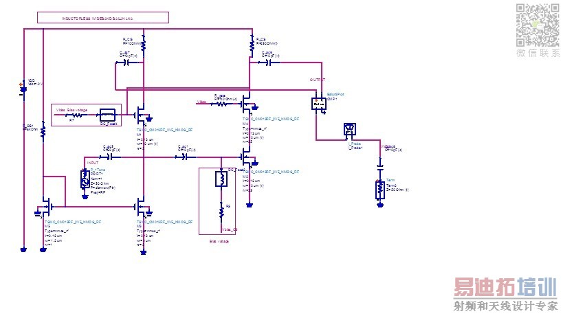
pls check this design..and pls suggest me for any mistakes and suggestions
You got 2 ports, where is the third one ?What does it mean "ports gain" ?
Sorry, have you ever designed any circuit in ADS ? ( or in any environment ) If you haven't,please start simpler ones.
Go through step-by-step to learn consistantly.
Check the signal path on the left side (M1/M2).
actually, i have connect external balun for S11,S22,S21,S12 results and later I have remove this balun and connected two output terminals.
I want to ask that in these two cases i got different gain result, so which gain result is correct,
case 1 with external balun--- gain(S21)= 8.3 dB MAX
CASE 2 with 3 terminals-- gain(S21)(RIGHT SIDE)=9 dB and gain(S31)(LEFT SIDE)= -19 dB. Whether i add these two gain S21+MAG(S31).
Do you understand that the left part of the circuit does (almost) nothing, and your circuit does not give the desired differential output signal?
For differential signal, both left and right stage must have the same gain.
申明:网友回复良莠不齐,仅供参考。如需专业帮助,请学习易迪拓培训专家讲授的ADS视频培训课程。
上一篇:ADS2011.10, is it supporting EM Simulation, When Circuit Contains SMT/SMD components
下一篇:cadence to ADS EM simulation
ADS培训课程推荐详情>>
 国内最全面、最专业的Agilent ADS培训课程,可以帮助您从零开始,全面系统学习ADS设计应用【More..】
- Agilent ADS教学培训课程套装
- 两周学会ADS2011、ADS2013视频教程
- ADS2012、ADS2013射频电路设计详解
- ADS高低阻抗线微带滤波器设计培训教程
- ADS混频器仿真分析实例视频培训课程
- ADS Momentum电磁仿真设计视频课程
- ADS射频电路与通信系统设计高级培训
- ADS Layout和电磁仿真设计培训视频
- ADS Workspace and Simulators Training Course
- ADS Circuit Simulation Training Course
- ADS Layout and EM Simulation Training Course
- Agilent ADS 内部原版培训教材合集