- 易迪拓培训,专注于微波、射频、天线设计工程师的培养
How to define port at EM
录入:edatop.com 点击:
hi everyone,
i have a Layout with EM and i want to generate it to EM symbol and connect Lumpresistors(pi attenuator) so i don't .
.know how to define my port because i have GND planes(2 layers) in the layout and the pi attenuator at the TOP layer
???how i need to define my port differential or with global GND
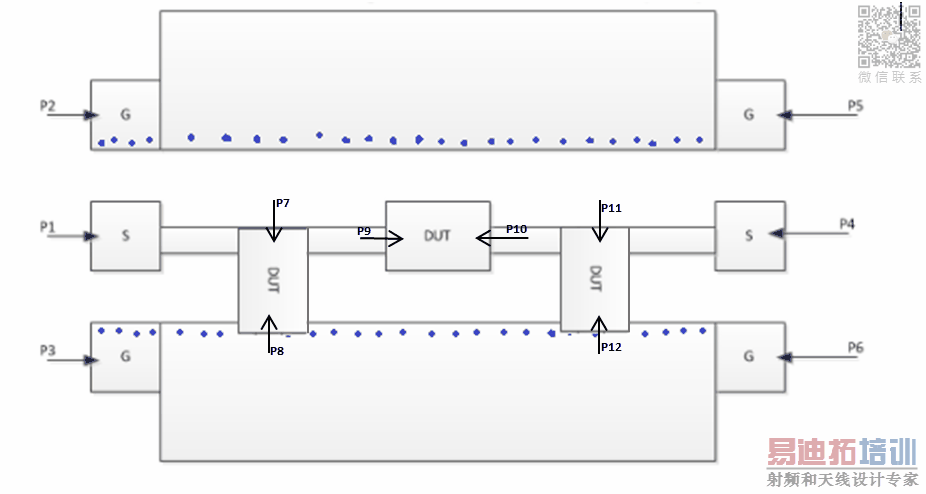
it's ok if I define the P7 positive and P8negative andP9positive and P10negative andP11 positive and P12negative.
Port1: P1 positive terminal, P2 and P3 negative terminals
Port2: P4 positive terminal, P5, P6 negative terminals.
in this illustrate i didn't use with global GND symbol and all the ports are diffirentials
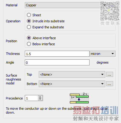
Note: the blue points they Vias ,connect the top GNDand the layer 2 and layer 3 GND and they are defined in the substrate like this
(in addition, the question is if the layers 2 and 3 need to be defined as a slot plane or like this(strip plane
regard,
aviad.
Hello,
if you draw the metal, then "strip" layer is correct.
Your understanding of port and is correct.
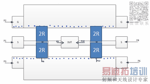
However, to keep symmetry, I would split each shunt resistor into two resistors (one to each GND).
Regards
Volker
thank you Volker for your response,
if I understand you right regarding to the resistors you mean to connect 1 of them to the ground on the other side but still with differential ports like the picture from my first post
and i have last question for multilayers stuckup, ,if i have line 50 ohm and in my layout i connect it to wider pad and ineed to openlayers only below thePad thus He will feel a different layer of GND, for example if the line 50 ohm on the Top layer and the wider pad connect to the line, so iopen below the pad6 layersbut only below the Pad
andnow i want to connectpins to the pad(like P1 P2 P3)and i'm asking you about the location of pins namely, if i need to connect thepins of the port on Top layer(where the Pad exists)or because i opened6 layers below the pad i need to connect them (minus pins) to layer7 becauseit is the GND for the Pad
regards,
aviad
Hi Aviad!
if I understand you right regarding to the resistors you mean to connect 1 of them to the ground on the other side but still with differential ports like the picture from my first post
Yes, I mean to have a total of 4 shunt resistors for symmetry, with the same total resistance. Connetion as additional differential ports and as you showed.
and ineed to openlayers only below thePad thus He will feel a different layer of GND, for example if the line 50 ohm on the Top layer and the wider pad connect to the line, so iopen below the pad6 layersbut only below the Pad
I didn't get this, can you explan again? I would make the phyiscal size (distance) as small as possible, so that you minimize transmission line effects within the attentuator pad.
andnow i want to connectpins to the pad(like P1 P2 P3)and i'm asking you about the location of pins namely, if i need to connect thepins of the port on Top layer(where the Pad exists)or because i opened6 layers below the pad i need to connect them (minus pins) to layer7 becauseit is the GND for the Pad
You should model the actual current flow in the hardware. Ground is where you connect ground return path. This looks like wafer probes connecting at top metal, so I would place my pins there at the top model, for measured/simulation agreement. In the final circuit, if your ground is on a lower layer, use that.
Best regards
Volker
申明:网友回复良莠不齐,仅供参考。如需专业帮助,请学习易迪拓培训专家讲授的ADS视频培训课程。
上一篇:Default mesh settings
下一篇:Modelithics Undefined Model Error in ADS2016.01
ADS培训课程推荐详情>>
 国内最全面、最专业的Agilent ADS培训课程,可以帮助您从零开始,全面系统学习ADS设计应用【More..】
- Agilent ADS教学培训课程套装
- 两周学会ADS2011、ADS2013视频教程
- ADS2012、ADS2013射频电路设计详解
- ADS高低阻抗线微带滤波器设计培训教程
- ADS混频器仿真分析实例视频培训课程
- ADS Momentum电磁仿真设计视频课程
- ADS射频电路与通信系统设计高级培训
- ADS Layout和电磁仿真设计培训视频
- ADS Workspace and Simulators Training Course
- ADS Circuit Simulation Training Course
- ADS Layout and EM Simulation Training Course
- Agilent ADS 内部原版培训教材合集