- 易迪拓培训,专注于微波、射频、天线设计工程师的培养
Distance between layout pin electrically large
录入:edatop.com 点击:
Hi everyone,
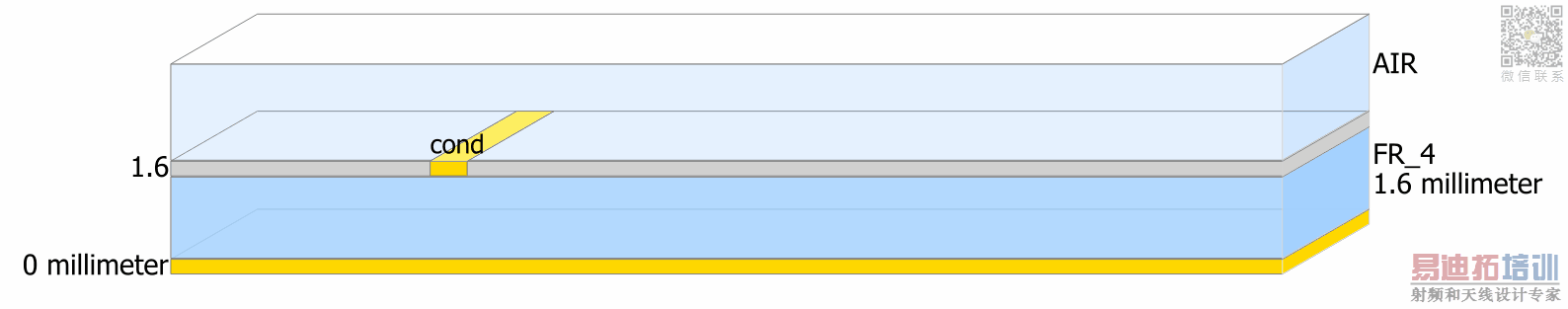
I'm just starting to use Momentum and I'm trying to perform a simple simulation of a microstrip matching network. The problem is that I'm getting that error when simulating, and the result doesn't seem accurate, especially at high frequencies, when compared to the circuit simulation. I'm using standard FR4 substrate, Er 4.5 and 1.6 mm thickness, 35 micron of conductor. My ports have been defined as "single" which I think that may be the reason of the error, but I'm neither sure if it's correct, nor able to change it to differential. I'm simulating from 100 MHz, to 10 GHz.
Thank you very much in advance
Can you show more details of your model?
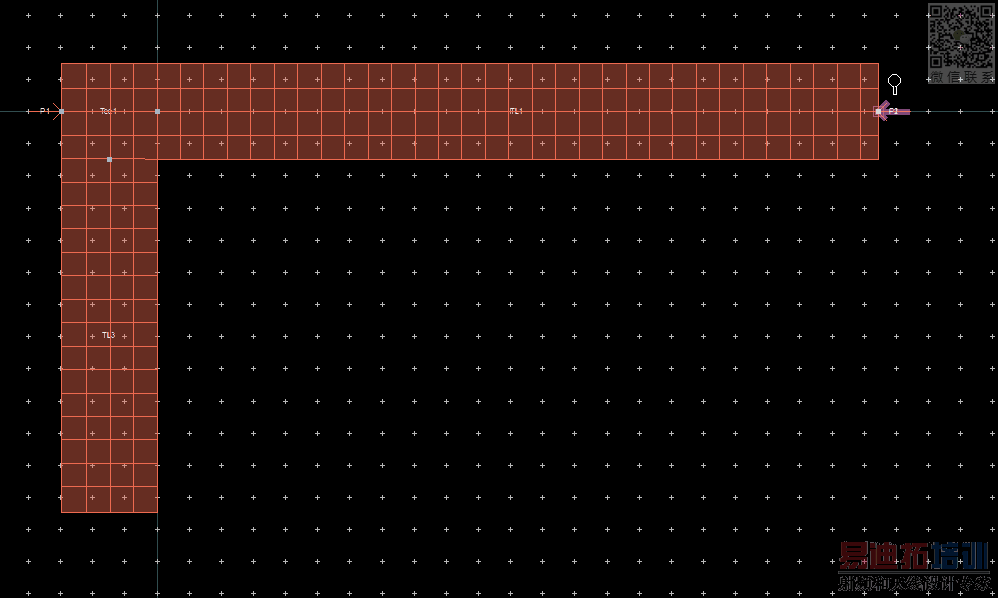
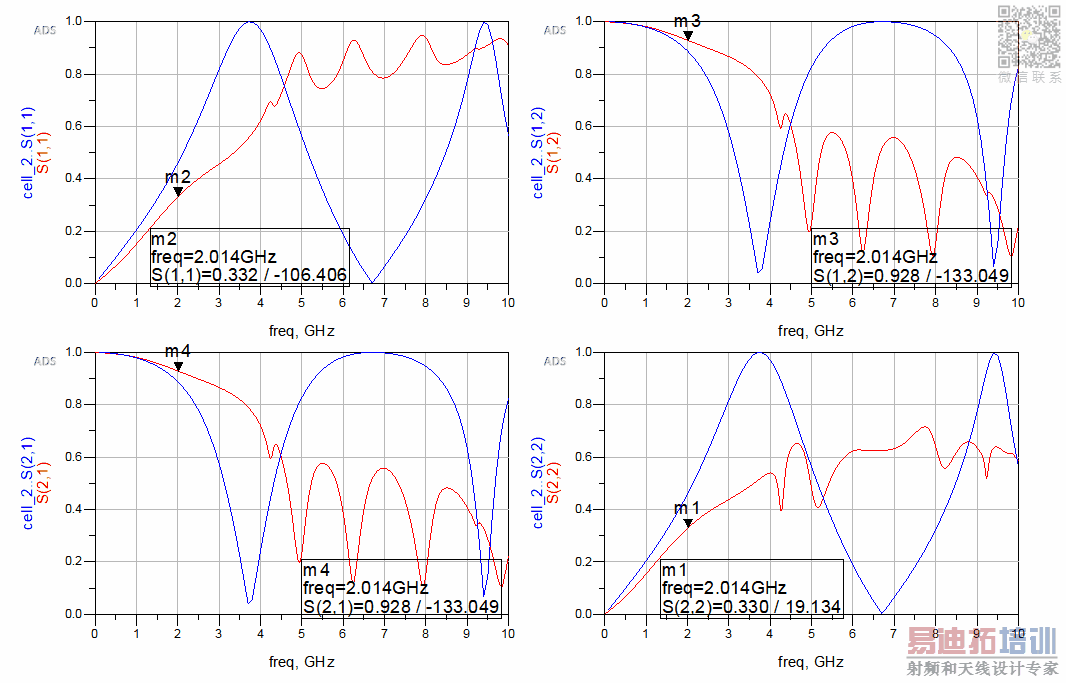
Sure, it's very simple, just stub and line. Indeed, the results don't seem correct, I attach them too. (blue, circuit simulator, red, momentum).
Thank you again!
I assume you used Momentum Microwave mode
What are the dimensions? The open stub with this thick substrate will cause radiation, which is not included in the circuit model.
Yes, I'm using Microwave Mode as I'm working in GHz, it is correct, isn't it?
Regarding dimensions, the width of both lines is 2.97 mm, and the lengths are 10.98 mm for the stub and 22.43 for the line. You mean that an open stub with such a thickness is technically incorrect?
Microwave mode is correct in this case, because your structure will radiate heavily.
And that's also what causes trouble: your FR4 is much too thick for operation at 10 GHz, it will behave very different from the ideal lines that you simulated with circuit models. There might also be another issue with your port width on the left side (1). I will check that if you upload the workspace.
(1) see appnote on port size:
http://muehlhaus.com/support/ads-application-notes/edge-area-pins:Dr. Mühlhaus Consulting & Software GmbH » Edge/Area pins in Momentum EM simulation
In that case, I guess that I'm not getting reliable results at 10 GHz (which I don't really care, as the design is at 2 GHz), because of the substrate itself. However, results at lower frequencies don't seem really accurate neither, so I'm going to check the width thing you mention (by the way, why do you say that I might have an issue just with the left port, instead of both?).
In the meantime, just to be sure, I would be very pleased if you could check my substrate definition:
Thank you again, volker, I'm very new in ADS and I'm learning a lot!
Please, can you upload the archived workspace (or a copy where you delete all other stuff)? I want to check a few things, but today I'm too busy to build your model from scratch.
Left port width: because the left port is on an edge that consists of the line and the stub. I'm worried that ADS will use that entire 2.97mm + 11mm for the port width, which would be an issue even at 2GHz. So I want to check currents in the model, to see what happens. Instructions for user controlled port width is in my appnote, or you just add a little bit of 2.97mm line before the stub, so that the port "sees" 2.97mm width at the port.
Of course, I am not sure if this is what you mean, but I attach my workspace in .7zads format. (cell 2 is the one under discussion).
That workspace is the last version, which I have just updated using a rectangle as port, following (in some way) the instructions of the link you gave me. I've got much more acceptable results below 5 GHz, you can see it yourself. Not sure if it's completely correct anyway.
附图/附件
Thanks, that's exactly the archived project I was asking for.
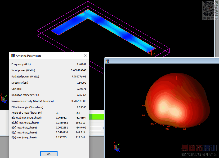
I've made the area ports a bit smaller (edge ports using a line with zero area would be another possibility), and results agree nicely with the circuit model at low frequency. As frequency increases, radiation also increases, and the line is acting as an antenna.We can see that from the power loss, calculated from the sum of squares of transmitted and reflected wave:
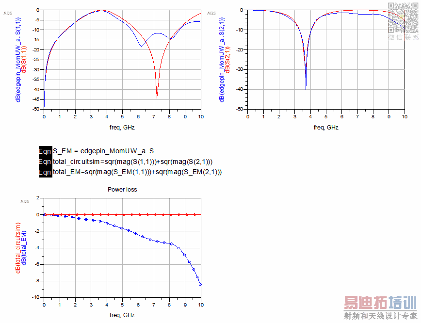
We can also look at the antenna gain ;-) of your line: -2.2dBi
So the difference in results is mostly physics: the line width thick substrate radiates, whereas the circuit model does not accout for radiation of the line.
My update to your model is attached.
Best regards
Volker
附图/附件
I'm just amazed! These are great results and great explanation, thank you very much again. Let me abuse of your help with one last silly question: Why don't insertion losses (-20log(|S21|)) coincide with the total losses you have just calculated?
Edit: I said it wrong, obviously they cannot coincide because they are different things, the strange thing for me is that total losses you calculated are way lower than insertion losses, when it should happen the other way around, shouldn't it?
Looking at my equation, I think I should have put db(srqt( sqr(|S11|) + sqr (|S21|)) there, because ADS dB() plot assumes voltages.
But to answer your question: My calculated loss is dissipated power, which is different from S21.
transmitted power + reflected power + dissipated power = incident power = constant.
In a lossless network, there is no dissipated power, and low S21 corresponds to high reflection. In this case power isn't lost=dissipated, it's just reflected. In the lossless network, we have: transmitted power + reflected power = incident power = constant. This is also seen in the circuit simulation: S11=0 where S21=1 and vice versa, and the calculated dissipation is 0. But for your EM simulated line, you will notice that power "disappears" by radiation, and that's a real effect caused by the thick substrate (thick in terms of wavelength).
Everything's clear, thank you very much for your generous help, I've learnt a lot with this thread. Best regards!
申明:网友回复良莠不齐,仅供参考。如需专业帮助,请学习易迪拓培训专家讲授的ADS视频培训课程。
上一篇:How I can freely modify the substrate in ADS?
下一篇:Model Kits bundled with ADS
ADS培训课程推荐详情>>
 国内最全面、最专业的Agilent ADS培训课程,可以帮助您从零开始,全面系统学习ADS设计应用【More..】
- Agilent ADS教学培训课程套装
- 两周学会ADS2011、ADS2013视频教程
- ADS2012、ADS2013射频电路设计详解
- ADS高低阻抗线微带滤波器设计培训教程
- ADS混频器仿真分析实例视频培训课程
- ADS Momentum电磁仿真设计视频课程
- ADS射频电路与通信系统设计高级培训
- ADS Layout和电磁仿真设计培训视频
- ADS Workspace and Simulators Training Course
- ADS Circuit Simulation Training Course
- ADS Layout and EM Simulation Training Course
- Agilent ADS 内部原版培训教材合集