- 易迪拓培训,专注于微波、射频、天线设计工程师的培养
Power divider simulation on ADS2011
录入:edatop.com 点击:
Hi everyone,
I’ve created a power divider on layout, when I use the component from the library on the schematic and do the simulation, I get an error message.
I don't know how to solve it.
Can anybody help me?
Thanks for replying.
Jefferson
I’ve created a power divider on layout, when I use the component from the library on the schematic and do the simulation, I get an error message.
I don't know how to solve it.
Can anybody help me?
Thanks for replying.
Jefferson
附图/附件

layout_power divider.jpg

schematic_power divider.jpg

simulation_error.jpg
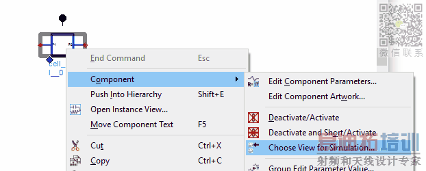
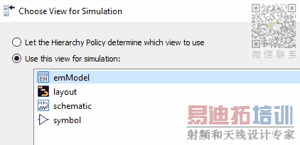
Jeff, you need to change the simulation view for the divider subcircuit cell10b1 from "schematic" to "emModel".
Hi,
How do I do it?
Could you describe the steps, please?
Thanks a lot, Volker!
Here are two screenshots to show the settings
附图/附件
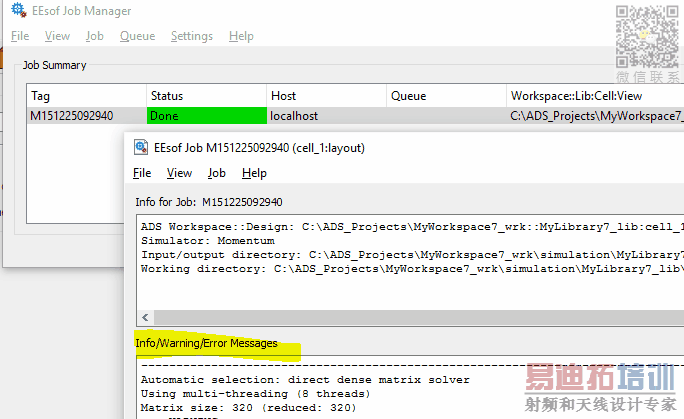
I've changed the simulation view to emModel, but I get this error message when I do the simulation.
Do you know why?
Thanks for replying.
Jefferson
jefferson90 on Dec 24, 2015 8:26 AM
附图/附件

error_simulation.jpg

schematic_divider.jpg
My understanding of the circuit simulation log messages is that there was an error when running the Momentum simulation. You might see more details in the Momentum log.
Does the Momentum simulation finish properly when started manually?
附图/附件
One more comment on your "ground" pins: the location of the ground reference matters, similar to the real hardware. You should place ground pins close to the signal pin.
You might also consider using defined size for the ground pins:
http://muehlhaus.com/support/ads-application-notes/edge-area-pins
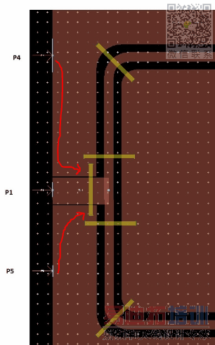
This is the message of simulation in momentum. I believe that all the pins are on the edge.
I am doing the power divider with CPW transmission line. You can see how I define the ports
I don't know how to solve it.
Thanks for replying.
Jefferson
附图/附件

ports layout.jpg

ports.jpg

momentum_simulation_error.jpg
> I believe that all the pins are on the edge.
> I am doing the power divider with CPW transmission line. You can see how I define the ports
Yes, and what I see is wrong. The ground pins must be at the edge near the signal conductor, not so far away as you have placed them. The ground current will flow at the edge of the conductor, at the gap. The position where you have placed the pin inserts a large extra path length.
For the error message, I think that is related to placement of ground pins (multiple pins on same edge on output side). You should contact Keysight support for help.
附图/附件
If you can see, the message of simulation in momentum says that there are warnings with the ports 10 to 13.
Do you say than the other ports are badly located too?
About the error message, I've tried to split the conductor in 2 parts, each one with a ground port, like the image but I get the same error.
Thanks for replying.
Jefferson
附图/附件

ports layout.jpg
> Do you say than the other ports are badly located too?
From more than 15 years experience as an EM simulation expert, yes, all ports placements look wrong to me.
申明:网友回复良莠不齐,仅供参考。如需专业帮助,请学习易迪拓培训专家讲授的ADS视频培训课程。
上一篇:How can I calculate the average value of an envelope in Ptolemy?
下一篇:De-embedding of cable with connectors in ADS for S-parameter
ADS培训课程推荐详情>>
 国内最全面、最专业的Agilent ADS培训课程,可以帮助您从零开始,全面系统学习ADS设计应用【More..】
- Agilent ADS教学培训课程套装
- 两周学会ADS2011、ADS2013视频教程
- ADS2012、ADS2013射频电路设计详解
- ADS高低阻抗线微带滤波器设计培训教程
- ADS混频器仿真分析实例视频培训课程
- ADS Momentum电磁仿真设计视频课程
- ADS射频电路与通信系统设计高级培训
- ADS Layout和电磁仿真设计培训视频
- ADS Workspace and Simulators Training Course
- ADS Circuit Simulation Training Course
- ADS Layout and EM Simulation Training Course
- Agilent ADS 内部原版培训教材合集