- 易迪拓培训,专注于微波、射频、天线设计工程师的培养
How to add pads/pins/names to GDSII layout for SIPro simulation?
录入:edatop.com 点击:
Dear all,
I am trying to perform SIPro simulations on a redistribution layer. This is essentially a single layer TSV to BGA pad fanout, etched on the bottom of a silicon chip. I will try to illustrate some things with images, but to protect customer IP, I need to be selective. Hopefully the explanations are sufficient.
The layout is imported from a GDSII file, with a top-level hierarchy as shown below. On the top level, there is an instance of BGA_PADS, which contains a 10x10 array of PADs (circular polygons). On the top level, there also is an array of TSVs (circular polygons). Finally, there are polygons which are the fan-out traces. The BGA pads, TSVs and traces all exist on one common copper layer (the pads and TSV also exist on other layers, but I ignore those layers for now). There are no net names or ports defined in the GDSII import.
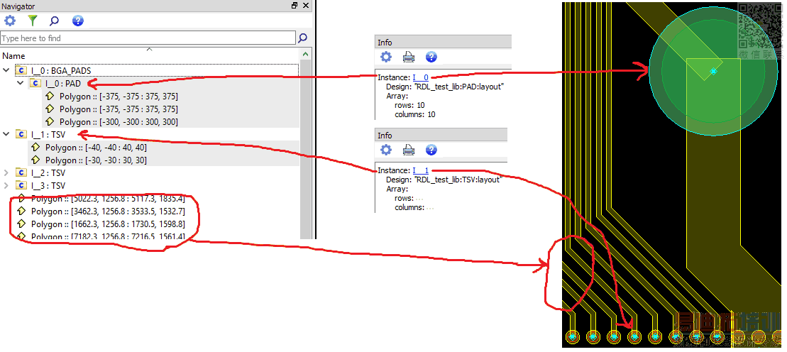
When importing this layout in SIPro/PIpro, the following happens (see below). The traces are correctly imported, but the BGA pads and vias are not. Moreover, the BGA_PADS shows up as a single instance I_0 without pin. The TSV shows up as an array of instances, but also without pins.
My question is threefold, but probably they are interrelated.
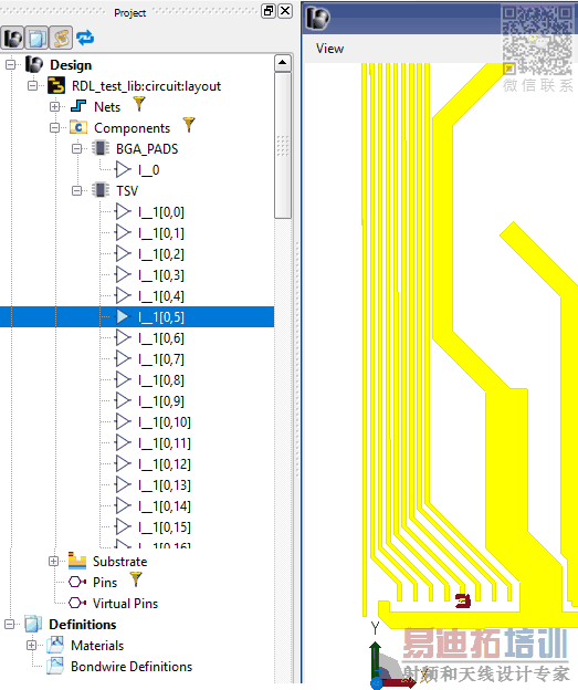
- How do I include the pads in the SI simulation? One solution that worked was to 'Flatten' thecomponents in layout: the compact 10x10 array is transformed in a list of 300 polygons. For SI simulation, this is good, but what if I need to change the pad size one day? Is there really no other solution?
- How do I add pins to the SI simulation? One solution that kind of worked, was to add a port to the TSV primitive, but this yielded a list of ports with names like I_1[0,7]_P1 and also seemed to connect to the same net. Probably, this is not the right way to do it.
- How do I add signal names to the SI simulation? One solution that kind of worked, was to add net names to the trace polygons, but probably there is a proper way to do this. Ideally, I would like assign signal names to the TSVs, because in the actual design, this is fixed (whereas the BGA pinning is still open for changes). The interconnects and BGA pads should then deduce their nets from connectivity with the TSVs.
Thanks in advance for your time and attention,
Sjoerd Op 't Land
Dear Sjoerd,
This issue will be dealt with by one of our tech support engineers. You will receive a notification by e-mail on how to access this case on our support portal.
Herman.
申明:网友回复良莠不齐,仅供参考。如需专业帮助,请学习易迪拓培训专家讲授的ADS视频培训课程。
上一篇:Extracting pilot signal
下一篇:Display - subtracting an array calculated from multi-dimension data
ADS培训课程推荐详情>>
 国内最全面、最专业的Agilent ADS培训课程,可以帮助您从零开始,全面系统学习ADS设计应用【More..】
- Agilent ADS教学培训课程套装
- 两周学会ADS2011、ADS2013视频教程
- ADS2012、ADS2013射频电路设计详解
- ADS高低阻抗线微带滤波器设计培训教程
- ADS混频器仿真分析实例视频培训课程
- ADS Momentum电磁仿真设计视频课程
- ADS射频电路与通信系统设计高级培训
- ADS Layout和电磁仿真设计培训视频
- ADS Workspace and Simulators Training Course
- ADS Circuit Simulation Training Course
- ADS Layout and EM Simulation Training Course
- Agilent ADS 内部原版培训教材合集