- 易迪拓培训,专注于微波、射频、天线设计工程师的培养
FEM-simulations to account for Ground-Inductances
录入:edatop.com 点击:
Transistors (active die) are embedded in ever more sophisticated packages.
These packages (eg QFN-type) are then soldered on top of a PCB.
We use FEM simulations to account for all impedance transformations due to the passive connections.
The most important is the added source-inductance because of the via-farm in the PCB underneath the QFN and in the embedded ground coin of the QFN package itself.
Usually the FEM simulated EM effects of the packaging environment and the active model of the transistor are combined in a schematic and then used together for Harmonic Balancing or S-parameter simulations.
We can understand that the S-parameters resulting from the FEM simulation account for the added Ground Inductance effect. However, thereisa myriad of possibilities to generate look-alike components with pins and to connect the active model to one-another. What are the best practices here?
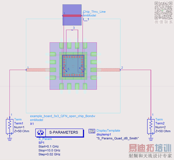
Under the FEM examples that come with ADS, there is an example workspace QFN_Designer_wrk.
In this example, theQFN package does not contain an active transistor, but a simple uStrip line. This makes a comparison with a simulation of the full layout easy and it allows us to ponder about the pinning and the porting.
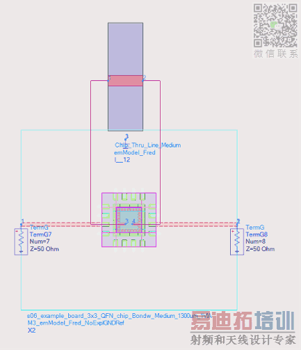
The uStrip-line is simulated in a separate, simple 2-port Momentum Simulation.Then, therest of the problem (with 2wirebonds)is simulated in FEM. In this latter setup, 2 single-ended ports are defined to global ground at theedges of the problem, and additionally, two internal differential ports are configured inside the QFN package and the line removed. See fig Keysight_embedding.png.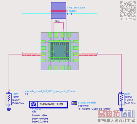
Note the double pins for the Differential portsin the QFN-lookalike layout. Note how the explicit gnd pin of the uStrip look-alike symbol of the uStrip line was added and how that pin is connected to the reference pins of both differential ports.
Original example
I ran these simulations and compared it with the full-wave 2-port simulation and noticed an important discrepancy.
That's when I started playing with the ports. This is what I did:
1st attempt
I undid the differential definition of the internal ports in the QFN-sectionand just considered each pin as a single-ended port, each referenced to the global gnd. Then the S-parameters aligned. This excellentreference:https://muehlhaus.com/support/ads-application-notes/em_line_ground(https://muehlhaus.com/support/ads-application-notes/em_line_ground)explains how differential ports only let the differential current circulate, while the 6-port single-ended approach is the more universal definition.
2nd attempt
I removed the two reference pins from the QFN-section all together and hence simulate the QFN section with only 4 SE-ports. Thus, the layout lookalike has 4 pins and I connect them like below. S-parameters lined up very well. Note how the explicit gnd-pin of the uStrip lookalike symbol is connected to global ground!This may throw off many, because if the uStrip were a transistor, they don't want to connect the gnd of the transistor to global ground, the entire idea to study the effect of the source-inductance isthat the gnd potential of the transistor gets offset from the global gnd!
Well, that is not how S-parameters work, as argued in the mentionedreference(https://muehlhaus.com/support/ads-application-notes/em_line_ground),
if we want to calculate thevoltage drop on the ground conductor, between port1 reference pin and port 2 reference pin, we can’t do that. There is no such information available in our 2-port data. Take a second to realize that, it’s important.
The underlying reason is the concept of Port Regularity, as discussedhere(https://ibis.org/summits/feb18/dmitriev-zdorov.pdf). Since S-parameters don't express the voltage drop between the references of the ports, you might as well consider them floating relative to one-another and therefore, there is nothing wrong with hanging all ports to global ground. The effect of Ls will be accounted for though, since the voltage in port 3,presented by that internal port to the active device, will be a reduced version of the input voltage. I tried this by replacing the uStrip by an active transistor.
3rd attempt
I kept the differential definition of the ports in the QFN-section and next simulated the uStrip section as a differential problem: removed the infinite ground and mapped a cond-layer as the gnd. At each end of the uStrip, I added a pin on that layer and defined those as the minus - sign of the ports at each respective end of the uStrip. Thus, the layout-lookalike has2 pins on each end of the line. See fig. Keysight_embedding_Diff.png. Here too, the S-parameters align very well.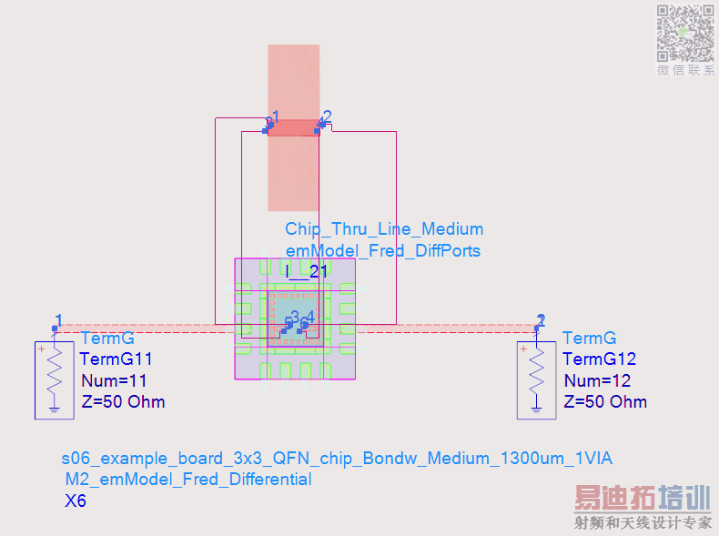
From my understanding, according to the mentionedreference,the approach in Original Example should yield correct S-parameters because even if you connect the references of both differential ports to the samepotential, the differential current will still flow: The 2-port model (result) with differential ports is “immune” to non-differential currents, and all current that flows into the signal conductor will return through the return path, no matter what else we try at schematic level.
So, why is it that the S-parameters correlate poorly? I admit that this 4-port problem is not exactly the same as the situation in the reference, but I am trying to extrapolate my understanding of it to this QFN problem.
It seems like you have to connect SE-ports with SE-ports and Differential ports to Differential ports in order to get correct S-parameters.
What am I still not understanding here?
Thanks for any help/discussion.
Hello Frederik,
interesting findings, I agree that something is wrong with this ADS example!
You wrote "From my understanding, according to the mentionedreference,the approach in Original Example should yield correct S-parameters" and that's true.
The partitioning approach including the port setup is correct, and we do get the correct response for the divided model (very close to all-in-one full EM) when using this black-box testbench instead of the look-alikes:
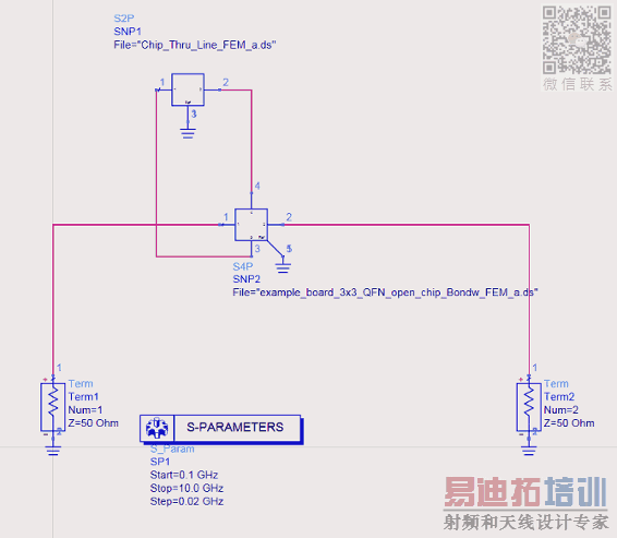
Whereas as look-alike testbench in the ADS example, which is supposed to model the same thing, provides different results. Note that it is exactly the same data, just using proper S2P and S4P as opposed to the look-alike connections!
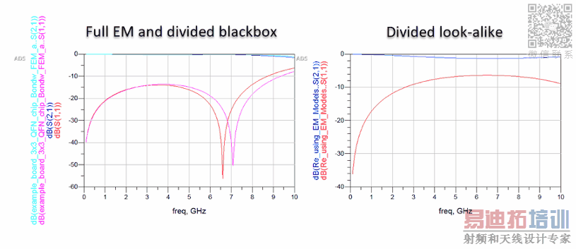
Conclusion: There is some issue with getting correct data when using the look-alikes!
I must admit that I'm scared by the look-alike in this situation because it pretends to offer freedom of wiring - which isn't real because the data behind the scenes used differential ports and thus ground connections are very limited in how they can/must be connected.
The EM data of both parts is fine, as seen by my testbench with S2P and S4. It is only the look-alike wiring of the exact same data that introduces some issue here. I'm not sure what that issue is, the netlist isn't very human-friendly to read.
Best regards
Volker
PS: unrelated to the topic above, there seems to be another issue with data sets messed up in the example: the initial result of the "Re_using_EM_Models_a" was 4-port data and there are more dataset with suffix _a and _c which indicate that the data supplied in the example is from FEM and not from this schematic testbench. I had to re-simulate to get the 2-port testbench dataset.

Dear Dr. Muehlhaus,
Thanks for your feedback. Good to know that I am on the right track with my thinking.
Is it advisable to use differential ports for these kind ofcases in the first place?
Like I pointed out, the single-ended ports give me the same results in fact.
Is that because the integration of the E-field in a single-ended port along an integration line to calculate the voltage basically yields zero when that integration line runs through metal?
Do you know if Keysight has more documentation on what exactly happens in a port? I find it not very well documented.
I also came across this interesting slide-deck about port regularity: https://ibis.org/summits/feb18/dmitriev-zdorov.pdf:https://ibis.org/summits/feb18/dmitriev-zdorov.pdf, which explains why the DUT that is being embedded in the simulated 4-port does not necessarily need to be offset from global ground in order to account for any source-inductance.
Thanks again.
Frederik
Hi Frederik,
all I know about these ports is from my own EM experience and understanding, so take this with a grain of salt:
internal ports with the reference at the physical in-package ground are sufficient, as long as there are no additional modes to care about. The more general model with all ports referenced to "global ground" will give the same results then, after using it in schematic with the actual wiring.
I suspect (not sure) that Momentum internally solves the "global ground" problem always, and the differential ports are a result of reducing that full S-matrix. I know that Sonnet does this, but for Momentum I am not sure.
One situation where the "global ground" ports would be preferred: if there can be additional modes that are not possible with the differential ports, i.e. common mode. But that doesn't apply to this example, in my opinion.
Do you contact Keysight regarding the issue with this example? I don't know if they will notice this discussion.
Best regards
Volker
Hello Dr. Muehlhaus,
Thanks for your reaction. I am in contact with Keysight on this through Dave Hunt.
I had a 1.5hour conversation with him last week. Not everything is clear yet, but here is (a short) summary of the progress I made with him:
1) Inthe Keysight logic,a port with an explicit ground pin is not a differential port necessarily; in ADS2020, in the port editor you can select per pin whether you want to make it differential and in the layout you will get 2 pins. I do not know what the difference between both is (yet). I did bring up theexample you haveon your website regarding differential ports and the unexpected results these may give(seeing an open if you connect the + pin to global ground) for example. He was going to look into that and discuss with other experts within Keysight.
2) In FEM (not sure about momentum), a port with explicit ground pin becomes either a rectangle or a triangle. (Triangle is best avoided and can be avoided by making edge-pins or making the layer a global gnd layer (from ADS2017 onwards)). But then that rectangle or triangle becomes an object thatis being meshed. So, at least in FEM, the resultingS-parameter matrixis not just a reduced version(where the differential mode in that port is withheld and the common mode is ignored)of the full-sizedS-parameter matrix with all single-ended ports.
3) On the example: Dave Hunt does recommend people using the explicit ground pin, but he had no explanation as to why the simulation results were worse with his recommendations than without. He was going to look into it.
I'll keep you updated.
Frederik
申明:网友回复良莠不齐,仅供参考。如需专业帮助,请学习易迪拓培训专家讲授的ADS视频培训课程。
上一篇:Schematics for non available ICs in the ADS library.
下一篇:Import IBIS model to ADS software
ADS培训课程推荐详情>>
 国内最全面、最专业的Agilent ADS培训课程,可以帮助您从零开始,全面系统学习ADS设计应用【More..】
- Agilent ADS教学培训课程套装
- 两周学会ADS2011、ADS2013视频教程
- ADS2012、ADS2013射频电路设计详解
- ADS高低阻抗线微带滤波器设计培训教程
- ADS混频器仿真分析实例视频培训课程
- ADS Momentum电磁仿真设计视频课程
- ADS射频电路与通信系统设计高级培训
- ADS Layout和电磁仿真设计培训视频
- ADS Workspace and Simulators Training Course
- ADS Circuit Simulation Training Course
- ADS Layout and EM Simulation Training Course
- Agilent ADS 内部原版培训教材合集