- ÒŚ”ÏÍŰĆàŃ”,ŚšŚąÓÚιȚĄąÉäÆ”ĄąÌìÏßÉèŒÆ耳ÌÊŠ”ÄĆàŃű
rfidÌìÏßșÍĐŸÆŹÆ„Ćä”ç·ÉèŒÆÎÊÌâ
ÂŒÈëŁședatop.com ”㻜Łș
ÇóžßÊÖ°ïĐĄ”ÜŽđÒÉœâ»óŁŹÔÚŚöĐŸÆŹșÍÌìÏßÆ„Ćäʱ”Ķ˿ڌèżčÓŠžĂÔőĂŽÉèÖĂ°Ą?
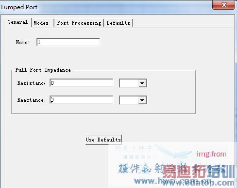
ŚèżčÉèÖĂÎȘĐŸÆŹŚèżč”ÄčČéî
ÏÂĂæÄÇžöŃĄÔńČ»čéÒ»»Ż
ÏëÎÊÒ»ÏÂŁŹŐâÖÖÇéżöÏžúÓĂĐŸÆŹÊ”ŚèżčŒ€Àűʱ»ń”Ă”ÄÔöÒæÒ»Ńù°ÉŁż°Ž”ÀÀíÀŽË”ŁŹÔöÒæÓŠžĂžúS11ÓĐčŰÏ””ÄŁŹÁœÖÖÇéżöÏ”ÄS11ÊÇČ»Ò»Ńù”ÄŁŹŐâžöÓŠžĂÔőĂŽÀíœâŁż¶àĐ»ŁĄ
Actually,I guess the gain you mentioned is the realized gain meaning how much gain you can really get after antenna is excited.
The realized gain depands on the directivity, the return loss (S11).
If the match network is off and your return loss is not low enough, then, that degrade your realized gain.
ÉêĂśŁșÍűÓѻ۞ŽÁŒĘŹČ»Æ룏œöč©ČÎżŒĄŁÈçĐèŚšÒ”Ń§Ï°ŁŹÇëČ鿎13.56MHz NFC/RFIDÌìÏßÉèŒÆĆàŃ”żÎłÌĄŁ
ÉÏÒ»ÆȘŁșčŰÓÚNFCÓĂÌúŃőÌć ČÄÁÏ
ÏÂÒ»ÆȘŁșALN-9662ŁšUHFŁ©±êÇ©ÌìÏßÉèŒÆ
13.56MHz ÏßÈŠÌìÏßÉèŒÆÏêÇé>>
 È«ĂæœâÎö 13.56MHz NFC/RFID ÏßÈŠÌìÏß”ÄÔÀíÓëÉèŒÆ, ÌìÏßÆ„Ćä”ç·”ÄÉèŒÆ”śÊÔ,ÒÔŒ°HFSS·ÂŐæ·ÖÎö”ÄÈ«čęłÌĄŸMore..Ąż
ÊÖ»úÌìÏßÉèŒÆĆàŃ”œÌłÌÏêÇé>>
 čúÄÚŚîÈ«ĂæĄąÏ”ÍłĄąŚšÒ””ÄÊÖ»úÌìÏßÉèŒÆĆàŃ”żÎłÌ,Ă»ÓĐÖźÒ»;ÊÇÄúŃ§Ï°ÊÖ»úÌìÏßÉèŒÆ”ÄŚîŒŃŃĄÔń...ĄŸMore..Ąż
ÎąĐĆč«ÖÚșĆ

ÉšĂè¶țÎŹÂëčŰŚąÎÒĂÇ”ÄÎąĐĆč«ÖÚșĆ
čŰŚąșóÊŚŽÎčșÂò±ŸŐŸżÎłÌżÉÏíÊÜŸĆŐÛÓĆ»Ę
ÌìÏßÉèŒÆÀžÄż
Æ””ÀŚÜĆĆĐĐ
- ADS·ÂŐæ13.56M PCBÌìÏß --ÓĐÍŒÓĐŐæÏà
- Ò»°ăPETÔÚ920MHzʱœé”糣Êę¶àÉÙŁż
- 13.56M RFIDÌìÏߔĎ«ÊäŸàÀëÈçșÎČâÊÔ
- łŹžßÆ”Óë”ÍÆ”ĄąžßÆ”RFID”çŚÓ±êÇ©”ÄÇű±đ
- RFIDÌìÏߌèżčĄąs11ČÎÊęÈçșÎČâ”ĂŁż
- 13.56mÌìÏß”ÄÖĐĐÄÆ”ÂÊÊÇ13.56mÂđŁż
- ÎąŽűÌìÏßÓĂSMAœÓÍ·șžœÓ
- rfid±êÇ©ÌìÏߎűżí”œ”ŚÒÔ-3dbÒÔÏ»čÊÇ-
- čŰÓÚ13.56MÌìÏß”ÄÎÊÌâ
- ÓĂHFSS·ÂŐæRFID±êÇ©ÌìÏß”ÄÎÊÌâ