- 易迪拓培训,专注于微波、射频、天线设计工程师的培养
CST2013 MWS Examples: Waveguide Junction
录入:edatop.com 点击:
Non-Optimized: | |
Optimized: |
General Description
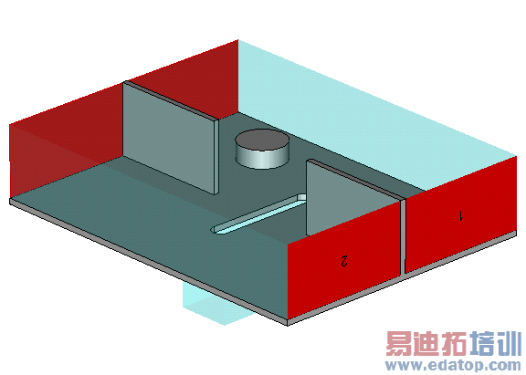
Here the S-parameter calculation of a waveguide hybrid junction is shown. The structure contains a coupling section with a small metallic disk and an external cavity resonator connected to the waveguides by a coupling hole. The definition of S-parameter symmetries enables the reduction of performed solver runs.
The structure is modelled by parametrical input and is used in two examples, as non-optimized junction and as optimized junction.
The optimized junction example applies the optimizer to tune the structure's parameters, so that the junction operates well at 8 GHz with low reflection at waveguide ports 1 and 2 and equal transmission to port 3 and 4.
Structure Generation
The structure is completely modelled by parametric input and thus can easily be modified. The single components of the device are created as bricks and cylinders, whereby identical parts are mirrored due to the symmetry of the structure. The edges of the coupling hole are smoothened using the blend facility.
Solver Setup
In order to enable a transient calculation four waveguide ports are defined, two at each side of the waveguide device, working as the excitation sources. Here the extension of the ports is specified by picking edge points. To examine the device over a broadband frequency range from 7 to 9 GHz the signal is determined as a Gaussian impulse.
Due to the symmetry of the structure the corresponding S-parameter symmetries are defined in the solver settings to save simulation time. In fact only one solver run is necessary to obtain all scattering parameters of the model.
In order to get a visualization of a monochromatic wave propagation a 3D monitor of the electric field is defined at the possible operation frequency. In addition, for the non-optimized example two voltage monitors are defined at the coupling hole and in the gap between the two waveguides to monitor the voltage over the time.
Optimizer Setup (only for optimized waveguide junction)
The goal of this optimization is to find a parameter settings which allows to operate the junction at 8 GHz with S31 = S41 = 0.707 and S11 and S21 as small as possible. The parameters considered for the optimization are listed here with its initial values:
Parameter Name | Initial Value | Description |
dh | 3.1 | disk height |
dr | 2.45 | disk radius |
g | 19 | gap size |
h | 11 | height of the waveguide |
w | 22.5 | width of the waveguide |
As optimizer type the Quasi-Newton optimizer with support of interpolation of primary data is chosen. The parameter intervals can be accessed in the optimizer dialog of the optimized example.
Post Processing
Both examples:
Performing a transient calculation using waveguide ports the resulting time signals are converted automatically into the desired scattering parameters. All these results are listed in the navigation tree in the folder 1D Results and demonstrate the wave propagation of the junction, indicating a proper excitation frequency for monochromatic operation.
Furthermore the results of the electric field monitor are stored in the folder 2D/3D Results, where also the calculated port modes of the given waveguide ports can be examined.
Compare the results of the optimized S-parameters to the non-optimized example, where the simulation is performed with the initial parameter settings of the optimization (see parameter box above).
Non-optimized example:
The voltages monitored at the coupling hole and in the gap between the two waveguides can also be accessed in the folder 1D Results.
Optimized example:
If the optimizer has finished the results of the last transient calculation (S-parameters, recorded fields, etc.) can be accessed through the navigation tree.
The optimized parameter settings can be found in the optimizer dialog box, the parameter list dialog box and in the optimizer logfile. In addition, information about the best goal function value and the course of the parameter variation by the optimizer can be found in this logfile.
CST微波工作室培训课程套装,专家讲解,视频教学,帮助您快速学习掌握CST设计应用
上一篇:CST2013 MWS Examples: Thermal Co-simulation: Electrical and Thermal Ana
下一篇:CST2013 MWS Examples: Threedimensional Waveguide Path
CST培训课程推荐详情>>
 最全面、最专业的CST微波工作室视频培训课程,可以帮助您从零开始,全面系统学习CST的设计应用【More..】
频道总排行
- Rectangular Waveguide Tutorial
- FSS: Simulation of Resonator
- CST2013 MWS Examples: Thermal C
- Dipole Antenna Array - CST201
- CST MWS Examples - CST2013 M
- Microstrip Radial Stub - CST2
- Dielectric Resonator Antenna -
- Interdigital Capacitor - CST20
- CST2013 MWS Examples: Biological
- Lossy Loaded Waveguide - CST2