- 易迪拓培训,专注于微波、射频、天线设计工程师的培养
Differential Via Pair - CST2013 MWS Examples
录入:edatop.com 点击:

General Description
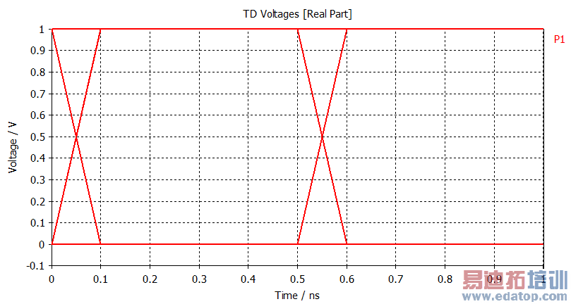
This example shows the calculation of a simple differential via pair. It analyses the eye-diagram using CST DESIGN STUDIO implementing Multipin-Ports and applying a pseudo-random bit-stream (PRBS). The model is created using simple shapes, curves, and different background layers.
Structure Generation
The vias and antipads are defined using cylinders, curves and other modeling features. The substrate and ground layers are defined by several PEC and dielectric layers in the 'Background' dialog using multiple background layers.
Solver Setup
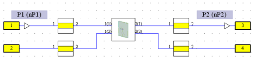
The excitation is done using Multipin-Ports within the waveguide definition. The simulation frequency is set to the range 0-20 GHz and field monitors are set for 10 GHz.
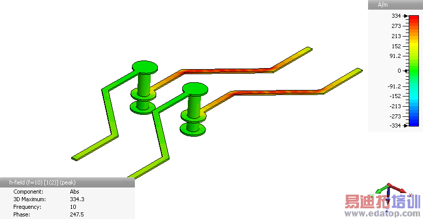
Post Processing
The time signals and S-parameters of the transient calculation are listed in the navigation tree in the folder 1D Results. You can further analyze the E-Field and the Surface Currents at 10 GHz.
The S-parameter results of CST MICROWAVE STUDIO are used to perform an eye-diagram simulation in CST DESIGN STUDIO using several ports, transmission lines, and a PRBS as a data signal.
The eye-diagram can be analyzed under the voltage results in the navigation tree:
|
|
Differential input | Differential output |

See also: Signal Integrity tutorial: Simulation of a Via Model
CST微波工作室培训课程套装,专家讲解,视频教学,帮助您快速学习掌握CST设计应用
上一篇: Branch Line Coupler - CST2013 MWS Examples
下一篇: Coax To Waveguide Transition - CST2013 MWS Examples
CST培训课程推荐详情>>
 最全面、最专业的CST微波工作室视频培训课程,可以帮助您从零开始,全面系统学习CST的设计应用【More..】
频道总排行
- Rectangular Waveguide Tutorial
- FSS: Simulation of Resonator
- CST2013 MWS Examples: Thermal C
- Dipole Antenna Array - CST201
- CST MWS Examples - CST2013 M
- Microstrip Radial Stub - CST2
- Dielectric Resonator Antenna -
- Interdigital Capacitor - CST20
- CST2013 MWS Examples: Biological
- Lossy Loaded Waveguide - CST2