- 易迪拓培训,专注于微波、射频、天线设计工程师的培养
Dual Patch Antenna - CST2013 MWS Examples
录入:edatop.com 点击:
General Description
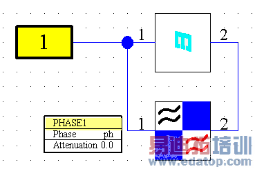
This example shows the calculation of S-Parameters, near- and far-fields of a dual patch antenna. Major point of this example is the demonstration of the capabilities of using the CST DESIGN STUDIO schematic in order to check the influence of amplitude and phase variations on the farfield pattern.
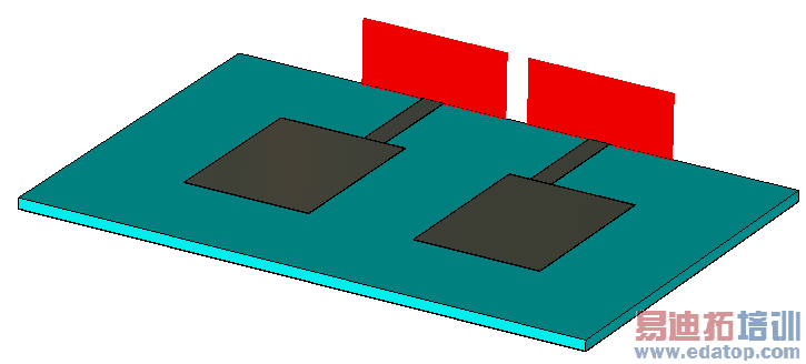
Structure Generation
The antenna and substrate are created using basic bricks. After the first patch and feed have been modeled, the second patch can be obtained by mirroring and copying the first one.
Solver Setup
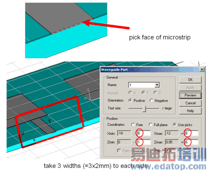
Two waveguide ports are defined using the picked face and port extension into free space and substrate by entering the numbers manually:
The Transient Solver is started with Ports=all setting. Please note, that the required independent port runs can be distributed to different machines using the Distributed Computing functionality.
Post Processing
The simulation delivers the farfields for the single excitations [1] and [2]. Switching to the schematic allows to study the phase variations very quickly. For this purpose an ideal phase shifter is used. It adds the specified shift to the results obtained by the single excitations [1] and [2] at a fixed frequency.
The definition of the Simulation Task "S-Parameter" then allows to combine 3D fields and farfields. These fields can be accessed through Result Templates (defined in CST DESIGN STUDIO). The combined E, H-field and farfield patterns are labeled by the excitation string "[S-Parameters1]" in the CST MICROWAVE STUDIO result tree.
CST微波工作室培训课程套装,专家讲解,视频教学,帮助您快速学习掌握CST设计应用
上一篇: Dielectric Lens - CST2013 MWS Examples
下一篇: 3D Transmission Line - CST2013 MWS Examples
CST培训课程推荐详情>>
 最全面、最专业的CST微波工作室视频培训课程,可以帮助您从零开始,全面系统学习CST的设计应用【More..】
频道总排行
- Rectangular Waveguide Tutorial
- FSS: Simulation of Resonator
- CST2013 MWS Examples: Thermal C
- Dipole Antenna Array - CST201
- CST MWS Examples - CST2013 M
- Microstrip Radial Stub - CST2
- Dielectric Resonator Antenna -
- Interdigital Capacitor - CST20
- CST2013 MWS Examples: Biological
- Lossy Loaded Waveguide - CST2