- 易迪拓培训,专注于微波、射频、天线设计工程师的培养
EM-cosmulation vs. schematic results of the pcb board
录入:edatop.com 点击:
Hi, I am designing a power amplifier on the pcb board.
I want to see the impedance of the bias part(RF choke to the DC input terminal).
I've compared the results of schematic and em-cosimulation,
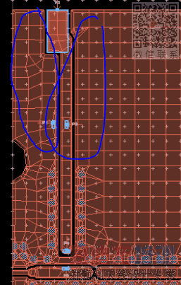
Layout.png
schematic.png
But the two results are quite different.(red is for em-cosimulation and blue is for schematic)
result2.png
You can see there is a knot on the red curve, and I am wondering if my em setup is right...
Here is the result of em simulation result(only for layout not em-cosimulation),and it looks strange...
result.png
Does anyone have any idea??
Thanks~
I want to see the impedance of the bias part(RF choke to the DC input terminal).
I've compared the results of schematic and em-cosimulation,
Layout.png
schematic.png
But the two results are quite different.(red is for em-cosimulation and blue is for schematic)
result2.png
You can see there is a knot on the red curve, and I am wondering if my em setup is right...
Here is the result of em simulation result(only for layout not em-cosimulation),and it looks strange...
result.png
Does anyone have any idea??
Thanks~
附图/附件

Layout.png

schematic.png

result.png

result2.png
In a grounded CPW, you need to connect the top ground plane to the bottom ground plane. These vias only exist near the thru line, but not in the vertical path. Current at C40 can only flow to the top ground, with no direct path (via) to the bottom ground. The short at the end of the line connects only to the bottom ground, but leaves the top grounds floating.
Check results after placing vias that connect the different grounds.
附图/附件
I have tried two ways to modify my layout.
The first way is to add vias along the bias transmission line, and the second way is to just add one via at the position of the ground pin of the bypass capacitor.
modified_layout.png
modified_layout2.png
Here is the em simulation result,where red curve is for many vias and blue curve is for one via.
But they look different.
modified_result1.png
Here is the em co-simulation result. They look the same,which overlap with each other, and the knot disappears, which look more accurate than the original result.
modified_result2.png
附图/附件

modified_layout.png

modified_layout2.png

modified_result1.png

modified_result2.png
Sorry,there is something wrong.
For the case of one via beside the ground pin of bypass capacitor, the result of em co-simulation still has a knot which looks strange
So only for the case of many vias along the bias line, the result is a smooth curve.
Hi volk:
Thank you for giving the advice. After I added the holes, the result became smooth and accurate.
But actually my real pcb board doesn't have these holes added afterwards, maybe the original result matches the measurement result???
> But actually my real pcb board doesn't have these holes added afterwards, maybe the original result matches the measurement result???
If the missing holes cause trouble in simulation, you should see the same effect in measurement, if the load impedance at the port is the same.
申明:网友回复良莠不齐,仅供参考。如需专业帮助,请学习易迪拓培训专家讲授的ADS视频培训课程。
上一篇:S21 data display with .s1p files and data items
下一篇:ADS Treatment of IBIS Models of Type I/O
ADS培训课程推荐详情>>
 国内最全面、最专业的Agilent ADS培训课程,可以帮助您从零开始,全面系统学习ADS设计应用【More..】
- Agilent ADS教学培训课程套装
- 两周学会ADS2011、ADS2013视频教程
- ADS2012、ADS2013射频电路设计详解
- ADS高低阻抗线微带滤波器设计培训教程
- ADS混频器仿真分析实例视频培训课程
- ADS Momentum电磁仿真设计视频课程
- ADS射频电路与通信系统设计高级培训
- ADS Layout和电磁仿真设计培训视频
- ADS Workspace and Simulators Training Course
- ADS Circuit Simulation Training Course
- ADS Layout and EM Simulation Training Course
- Agilent ADS 内部原版培训教材合集