- 易迪拓培训,专注于微波、射频、天线设计工程师的培养
How to set up a two-layer PCB without a ground plane on ADS
录入:edatop.com 点击:
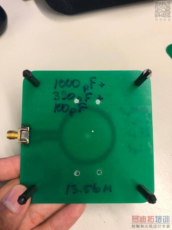
I am trying to module a one-turn coil in my lab on ADS, but I am confused by the complex parameters' setting. Attached are the pictures of the coil in my lab. It is a two-layer PCB. On the top layer, it has a one-turn coil, and there is nothing on the second layer. The substrate is FR4.
Continue...
I really don't know how to set up such a substrate on ADS. The attached screenshots here are how I define the substrate. I assume the top and bottom AIR Dielectric layers are just nothing. The FR4 Dielectric layer defines the substrate of the PCB. The Conductor Layer defines the copper trace of the PCB. Two strip planes on top and bottom of FR_4 are the top and bottom layers of the PCB. I am not sure if this is correct.
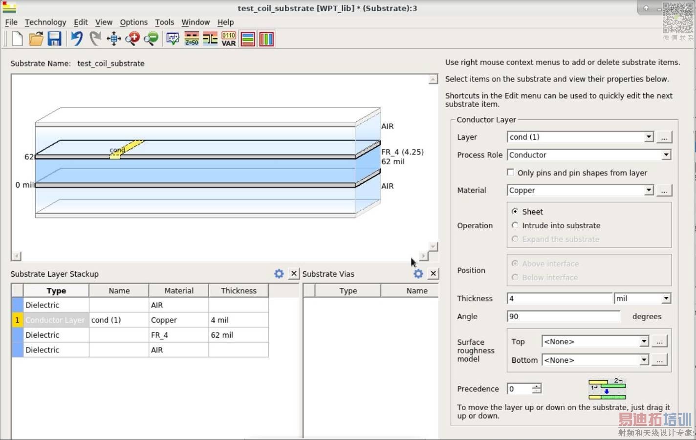


Another question is I do not know how to link the substrate in the layout here (cyan color) to the FR4 defined in the Substrate.

Hello,
your Momentum stackup definition is correct.
It also includes the definition for the dielectric layer, and because that is simulated as an infinite dielectric plane there is no need to map the dielectric boundary (PCB outline).
Other hints:
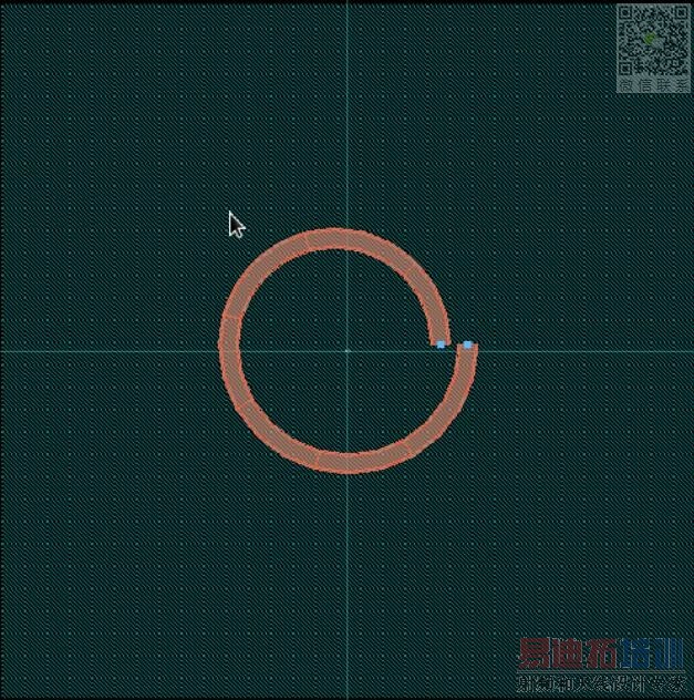
- In your EMsetup, go to Options > Preprocessor and change settings in the "Simplify the Layout" section to less agressive simplification. I would recommend 15 degrees instead of 45 degrees, to better keep the shape of the loop.
- For the ports, place a pin on each end of the loop and then combine that into a differential port by dragging pin 2 to the minus terminal of port 1. You then have a differential port where pin 1 is and pin 2 is
Good luck!
Volker
Dear Volker,
Thanks so much for your advances. Before running my simulation, could you help me check if I followed your advances correctly?

I also attached the screenshot of the setting of Options-Mesh

Looks good to me!
I am not sure if you are familiar with the behavior of S11 of spiral coils. My objective of designing the coil on ADS is finding its inductance, and then add capacitors to tune the resonant frequency to 13.6 MHz. However, the simulation result looks really odd to me.
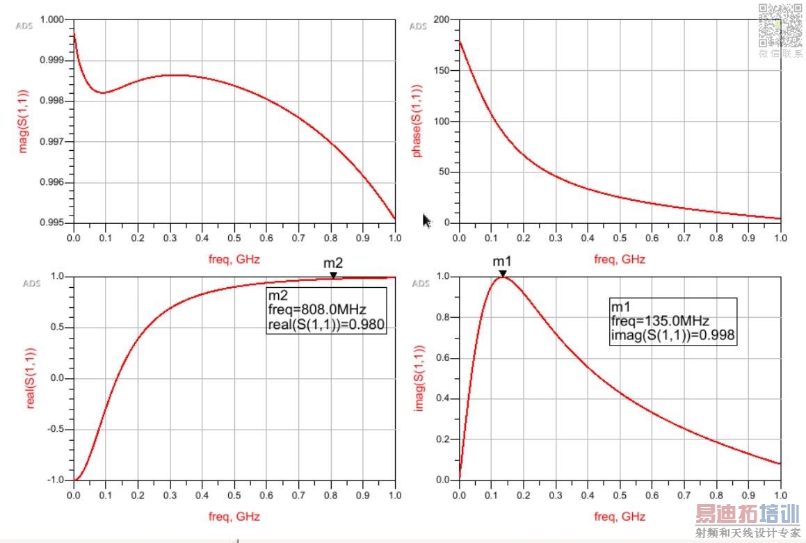
What I expect are:
mag(S11): Keep increasing due to the inductance of the coil before the self-resonant frequency. After it reaches the self-resonant frequency, it will negate the magnitude and start increasing until it reaches 0.
phase(S11): start from 0 to 180
real(S11): always a constant due to the small amount of parasitic resistance
imag(S11): similar behavior of mag(S11) due to its inductance before the self-resonant frequency and capacitance after the frequency
Yes, I am working a lot on spiral inductors. Your small loop is almost a perfect short.
To evaluate inductance, you can use equations as shown below.
I have also attached link where you can download the data display file (*.dds), please unpack to your workspace directory.

https://muehlhaus.com/wp-content/uploads/2019/10/inductance.zip:https://muehlhaus.com/wp-content/uploads/2019/10/inductance.zip
The inductance of mine is not a constant, which is kind of weird compared to your result. I also expect the inductance of the coil to be 95.7 nH, since the coil of my lab connected to capacitors (1.43 nF) to tune to the 13.6 MHz resonant frequency. I use the equation f = 1/2*pi*sqrt(LC) to derive that the L suppose to be 95.7 nH.
Any thoughts about it?
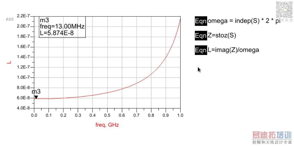
That increase towards SRF is expected for the "real" physical coil. My testcase was an ideal (schematic) inductor with flat L=1nH. Sorry if I caused confusion.
The difference in value should be resolved if you add the feedline (up to SMA) to your Momentum model.
The difference in value should be resolved if you add the feedline (up to SMA) to your Momentum model.
Ok, let me try it!
Actually, one thing that burned me tons of time was finding an accuratecomponent to module the coil. I cannot really find a coil that even similar to the one I have in my lab if I set the number of turn to 1.
For fixed artwork, you can draw it using polygons and circles (boolean operation to remove small circle from large circle).
Or maybe you can create something useful with the MCURVE element as well, plus some MBEND and MLIN.
Use with this appnote:
https://muehlhaus.com/support/ads-application-notes/em-parameters-momentum:Dr. Mühlhaus Consulting & Software GmbH » Using layout parameters in Momentum EM simulationshttps://muehlhaus.com/support/ads-application-notes/ael-artwork:
If you need your own scaled artwork, it's a bit more involved. Here are appnotes that I wrote on creating your own scalable artwork for EM:
https://muehlhaus.com/support/ads-application-notes/ael-artwork:Dr. Mühlhaus Consulting & Software GmbH » Create customized artwork cells using AEL code
https://muehlhaus.com/support/ads-application-notes/ads-miniaturized-bpf-ael:Dr. Mühlhaus Consulting & Software GmbH » Miniaturized Bandpass Filter (AEL layout example)
Sure thing! There is a lot of things I need to play around with now. I will try to create my own artwork and test it again. Again, I really appreciate your help!
I just want to let you know that I made it. The inductance of simulation is around 95.15 nH, and match my expected result 95.70 nH. Thanks again for your help! I really appreciate that


申明:网友回复良莠不齐,仅供参考。如需专业帮助,请学习易迪拓培训专家讲授的ADS视频培训课程。
上一篇:How do I deal with metals that intrude into multiple dielectric layers
下一篇:最后一页
ADS培训课程推荐详情>>
 国内最全面、最专业的Agilent ADS培训课程,可以帮助您从零开始,全面系统学习ADS设计应用【More..】
- Agilent ADS教学培训课程套装
- 两周学会ADS2011、ADS2013视频教程
- ADS2012、ADS2013射频电路设计详解
- ADS高低阻抗线微带滤波器设计培训教程
- ADS混频器仿真分析实例视频培训课程
- ADS Momentum电磁仿真设计视频课程
- ADS射频电路与通信系统设计高级培训
- ADS Layout和电磁仿真设计培训视频
- ADS Workspace and Simulators Training Course
- ADS Circuit Simulation Training Course
- ADS Layout and EM Simulation Training Course
- Agilent ADS 内部原版培训教材合集