- 易迪拓培训,专注于微波、射频、天线设计工程师的培养
Linear LTC2145-14低功耗125Msps 14位模数转换方案
录入:edatop.com 点击:
Linear公司的LTCR2145-14/LTC2144-14/LTC2143-14是低功耗" title="低功耗">低功耗
2路同时取样的14位模数转换器(ADC),SNR达到73.1dB,SFDR为90dB,取样速率达125Mbps,DC指标包括±1LSB INL, ±0.3LSB DNL,整个温度范围内不会丢失码,CMOS输出摆幅从1.2V到1.8V,主要用在通信,蜂窝基站,软件定义无线电(SDR),手提医疗图像设备,多路数据采集" title="多路数据采集">多路数据采集
和非破坏性测试.本文介绍了LTC2145-14主要特性, 功能方框图,典型应用电路以及输入频率" title="输入频率">输入频率
5MHz-150MHz, 150MHz-250MHz" title="250MHz">250MHz
和大于250MHz的前端电路图, 1620A演示板" title="演示板">演示板
电路图和材料清单(BOM).
The LTCR2145-14/LTC2144-14/LTC2143-14 are 2-channel simultaneous sampling 14-bit A/D converters designed for digitizing high frequency, wide dynamic range signals.
They are perfect for demanding communications applications with AC performance that includes 73.1dB SNR and 90dB spurious free dynamic range (SFDR). Ultralow jitter of 0.08psRMS allows undersampling of IF frequencies with excellent noise performance.
DC specs include ±1LSB INL (typ), ±0.3LSB DNL (typ) and no missing codes over temperature. The transition noise is 1.2LSBRMS.
The digital outputs can be either full rate CMOS, double data rate CMOS, or double data rate LVDS. A separate output power supply allows the CMOS output swing to range from 1.2V to 1.8V.
The ENC+ and ENC– inputs may be driven differentially or single-ended with a sine wave, PECL, LVDS, TTL, or CMOS inputs. An optional clock duty cycle stabilizer allows high performance at full speed for a wide range of clock duty cycles.
LTC2145-14主要特性:
Two-Channel Simultaneously Sampling ADC
73.1dB SNR
90dB SFDR
Low Power: 189mW/149mW/113mW Total 95mW/75mW/57mW per Channel
Single 1.8V Supply
CMOS, DDR CMOS, or DDR LVDS Outputs
Selectable Input Ranges: 1VP-P to 2VP-P
750MHz Full Power Bandwidth S/H
Optional Data Output Randomizer
Optional Clock Duty Cycle Stabilizer
Shutdown and Nap Modes
Serial SPI Port for Configuration
64-Pin (9mm × 9mm) QFN Package
LTC2145-14应用:
Communications
Cellular Base Stations
Software Defined Radios
Portable Medical Imaging
Multi-Channel Data Acquisition
Nondestructive Testing

图1.LTC2145-14功能方框图
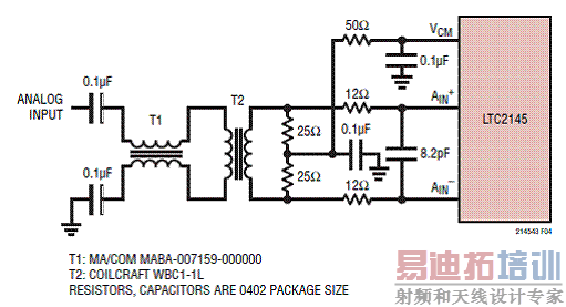
图2.LTC2145-14输入频率5MHz-150MHz的前端电路图
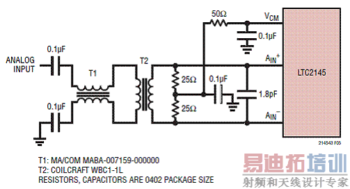
图3.LTC2145-14输入频率150MHz-250MHz的前端电路图
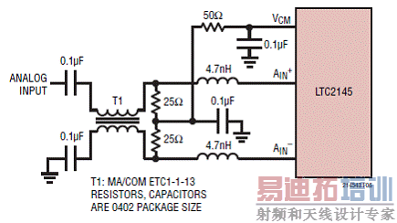
图4.LTC2145-14输入频率大于250MHz的前端电路图

图5.LTC2145-14采用高速差分放大器的前端电路图

图6.LTC2145-14典型应用电路图
1620A演示板
Demonstration circuit 1620A supports a family of 16-/14-/12-bit, 25Msps to 125Msps ADCs. Each assembly features one of the following devices: LTC®2185, LTC2184, LTC2183, LTC2182, LTC2181, LTC2180, LTC2145-14, LTC2144-14, LTC2143-14, LTC2142-14, LTC2141-14, LTC2140-14, LTC2145-12, LTC2144-12, LTC2143-12, LTC2142-12, LTC2141-12, or LTC2140-12 high speed, high dynamic range ADCs.
Demonstration circuit 1620A supports the LTC2185/LTC2145 family DDR LVDS output mode.
The versions of the 1620A demo board supporting the LTC2185 and LTC2145 series of A/D converters. Depending on the required resolution and sample rate, the DC1620A is supplied with the appropriate ADC. The circuitry on the analog inputs is optimized for analog input frequencies from 5MHz to 70MHz. Refer to the data sheet for proper input networks for different input frequencies.
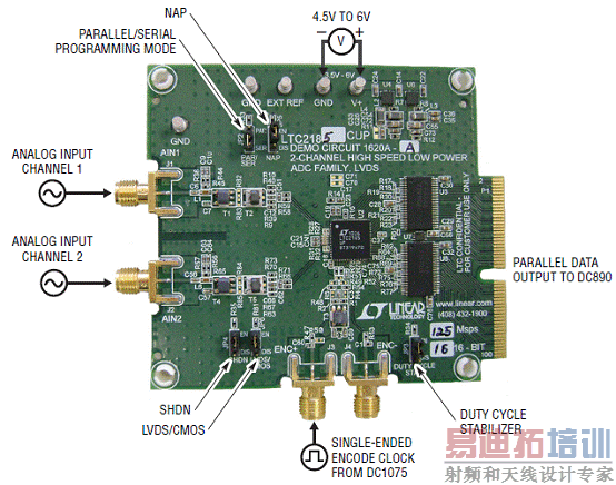
图7.1620A演示板外形图
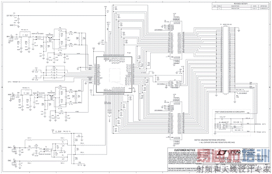
图8.1620A演示板电路图(1)
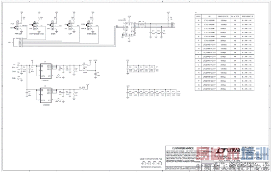
图9.1620A演示板电路图(2)
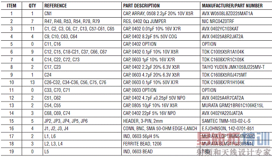
1620A演示板材料清单(BOM):

详情请见:
http://cds.linear.com/docs/Datasheet/21454314p.pdf
和
http://www.linear.com/demo/DC1620A-G
<script type="text/javascript" src=""></script><script type="text/javascript">show_share(1);</script>