- 易迪拓培训,专注于微波、射频、天线设计工程师的培养
并联电源管理芯片加速电源打开速度(英)
录入:edatop.com 点击:
In certain applications, design requirements may call upon a system’s switched-mode power supply to more promptly deliver its output than would the garden-variety power supply. 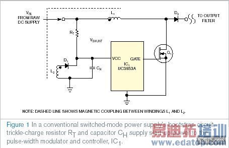
Resistor RT and capacitor CH form a trickle-charge circuit that supplies power for bootstrapping IC1 into normal operation. In conventional designs, RT comprises a high resistance that delivers just enough current to overcome the standby current and supply a trickle charge to holdup capacitor CH, which stores enough energy to power the PWM circuit until the power converter begins operation. Under normal circumstances, the circuit’s slow start-up response poses no problems.
When faster power-on response becomes important, you can reduce the bootstrap time by reconfiguring the start-up shunt regulator (
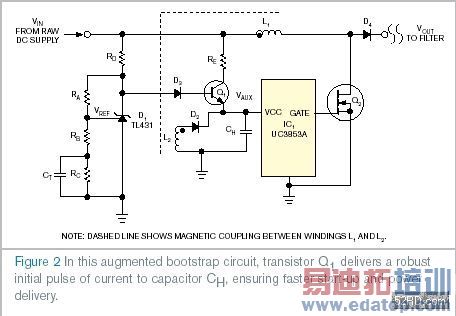
At turn-on, the VAUX voltage reaches its peak voltage, VAUX_PEAK, which the ratio of resistors RA and RB determines. Capacitor CT and resistor RC conserve energy by setting the bootstrap circuit’s turn-off time and voltage. Resistor RD supplies bias current to D1, the TL431 shunt-regulator IC, and resistor RE keeps transistor Q1 within its safe operating area by limiting its collector current.
To design the circuit, begin by selecting resistors RA and RB to establish the peak charging voltage, as the following equation shows:
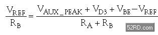
where VREF represents the TL431’s internal reference voltage. Next, select resistor RC to reduce the shunt-regulated voltage below the nominal VAUX voltage, VVAUX_NOMINAL, which the auxiliary winding supplies:
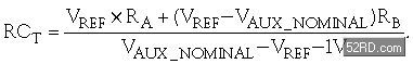
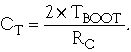
Choose capacitor CT’s value to set the bootstrap time, TBOOT, as follows:
As in Figure 1, diode D2 and auxiliary winding L2 provide normal operating power to IC1.
上一篇:回音消除技术
下一篇:输出阻抗怎么理解?多大比较好?