- 易迪拓培训,专注于微波、射频、天线设计工程师的培养
转换模式 PFC 提高效率以满足 80 以上的要求(英)
录入:edatop.com 点击:
Our world is rapidly changing into a global economy with an ever-increasing population of electronic consumers. We have more electronics in the home today per the average family than ever before. In the 1960s, home electronics in the US and Europe consisted of a television, oven, washing machine, refrigerator, simple power tools and probably a stereo system. Today the average home has all these items plus many more electronic gadgets that consume power such as high definition (HD) TVs, game systems, cellular phones and personal computers. What makes things even worse is that most homes have two or more of these new electronics — and all are consuming energy. Many of these devices are powered offline and not that efficiently. This wasted energy is depleting the world’s natural resources.
Countries around the world are now adopting standards to improve efficiency and to conserve energy. One of these standards is the 80+ initiative. This is where an offline power supply needs to have greater than 80 percent efficiency from 20 percent to 100 percent of the converter’s output power. These new standards are forcing power supply designers to find innovative ways to improve efficiency on new designs. This article will discuss how transition mode power factor corrected (PFC) boost pre-regulators can help power supply manufacturers meet these new efficiency requirements.
Problem
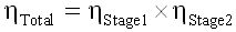
To help remove unwanted losses from the power lines, the European Union has enacted EN61000-3-2 standards for offline power supplies. These standards consist of harmonic current content specifications that apply to offline power supplies greater than 75 W. The most popular way for switching power supplies to meet these specifications is with an active power factor corrected boost pre-regulator followed by a step down converter (see Figure 1). Overall total system efficiency (η total) is the product of stage one’s efficiency (η Stage1) and stage two’s efficiency (η Stage1), which makes for an overall less efficient power supply.
Equation 1
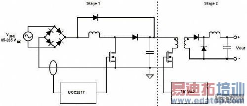
Figure 1: Two Stage Offline Power Supply with PFC Front End
Solution
One power factor correction pre-regulator technique being adopted to meet these new efficiency needs is to go from an average current mode boost to a transition mode boost pre-regulator. This PFC boost pre-regulator incorporates zero current switching to remove the reverse recover losses in the boost diode. The transition mode PFC pre-regulators have a zero current detect that waits for the inductor to completely de-energize before turning on the boost FET for the next switching cycle. Most of these converters use a constant on-time and vary the converters off-time to maintain the correct duty cycle. This is a pulse frequency modulation (PFM) that, when designed correctly, will have an inductor with a similar volume to the inductor used in an average current mode control pre-regulator with less switching losses from the semiconductor devices.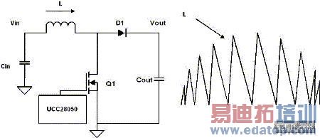
Figure 2: Transition Mode PFC Boost
Figure 3: Transition Mode Frequency vs. Line Voltage Phase Angle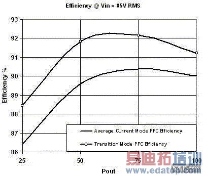
Figure 4: Low Line Efficiency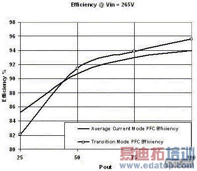
Figure 5: High Line Efficiency
One power factor correction pre-regulator technique being adopted to meet these new efficiency needs is to go from an average current mode boost to a transition mode boost pre-regulator. This PFC boost pre-regulator incorporates zero current switching to remove the reverse recover losses in the boost diode. The transition mode PFC pre-regulators have a zero current detect that waits for the inductor to completely de-energize before turning on the boost FET for the next switching cycle. Most of these converters use a constant on-time and vary the converters off-time to maintain the correct duty cycle. This is a pulse frequency modulation (PFM) that, when designed correctly, will have an inductor with a similar volume to the inductor used in an average current mode control pre-regulator with less switching losses from the semiconductor devices.
Figure 2: Transition Mode PFC Boost
Reduce switching losses without increasing inductor volume
To show that transition mode PFC pre-regulators can be more efficient, two 100W theoretical PFC boost pre-regulators for universal line applications are constructed and evaluated. The following table lists the design requirements of both pre-regulators.
|
Table 1: Specifications for Theoretical Boost Stage
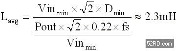
First, we select the boost inductor for average current mode (Lavg) with 22 percent inductor ripple current with a fixed switching frequency (fs) of 100 kHz. The average current mode boost inductor required for this design is roughly 2.3 mH.

Equation 2
Equation 3
Next we select a boost inductor for the transition mode PFC pre-regulator (Ltran). The inductor is selected based on a 25 kHz switching frequency at the peak of low line to design the power converter for the lowest switching frequency possible without the converter going audible. This low frequency is chosen to make the converter as efficient as possible. Under these constraints, the boost inductor required for the transition mode converter is roughly 1.0 mH.

Equation 4
To show that these inductors have similar volumes, a mathematical comparison of inductor area products (WaAc) is conducted. The following two equations describe the area product of the average current mode boost inductor (WaAcavg)) and the area product of the transition mode boost inductor (WaActran). In these equations ΔB is flux density, Cd is current density, and Ku is the magnetic winding factor. In this example, the value of these variables is the same for both designs. The exact value of these variables is not important.

Equation 5

Equation 6
In this example when evaluating the ratio of the area product of the transition mode to average current mode control, it is clear that the area products of both inductors’ magnetic cores are the same. This should result in the same boost inductor volume for both designs.
Equation 7
Losses
Boost diode reverse recovery loss (Pdiode_trr)
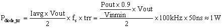
In average current mode boost pre-regulators, one of the highest losses to efficiency is the reverse recovery loss of the boost diode (Pdiode_trr). This loss is due to how long it takes to discharge (trr) the boost diode’s capacitance. In this theoretical design, the diode reverse recovery loss would be 1 W of loss — or roughly one percent of the total output power. A transition mode pre-regulator does not have this reverse recovery loss due to the zero current switching (ZCS) of the topology. This should result in a converter that is roughly one percent more efficient.
Equation 8
FET switching losses
The FET switching losses in a PFC boost pre-regulator (PFET_Switching) are generally quite large due to the high output voltage. Equation 9 can be used to estimate FET switching losses, where tr and tf are the FET’s fall and rise times respectively. These switching losses are at their peak at the minimum input voltage of the design.

Equation 9
The switching frequency of a transition mode PFC (fs(θ)) moves with changes in line and output power. The following equation and graph describe how the switching frequency of a transition mode boost pre-regulator changes with line at minimum input voltage and maximum load. In this application at low line, the switching frequency varies from 36 kHz to 25 kHz with changes in line voltage. The average switching frequency (favg) at low line is roughly 29 kHz. This is derived by taking the average switching frequency (fs) over half a line cycle.
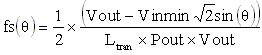
Equation 10
Figure 3: Transition Mode Frequency vs. Line Voltage Phase Angle
Figure 4: Low Line Efficiency
The average switching frequency (favg) of the transition mode converter is 29 kHz. The average switching frequency of this converter is roughly 29 percent of the fixed frequency approach. This reduced average switching frequency results in a 71 percent reduction in FET switching losses. In this example we can estimate the rise and fall times to be roughly 100 ns, and estimate that 1.4 W of FET switching losses (PFET_Switching) will be removed by going to a transition mode converter.
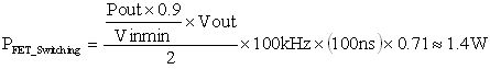
Equation 11
In this numerical example, 1.4 W of switching loss was removed by going from an average current mode control boost to a transition mode boost PFC pre-regulator. This results in roughly a 1.4 percent efficiency improvement. Theoretically, going from an average current mode control PFC pre-regulator to a transition mode pre-regulator could improve the efficiency of the converter by roughly 2.4 percent without increasing the boost inductor size.
To evaluate the efficiency improvements of transition mode PFC over an average current mode boost, two 100W PFC pre-regulators were constructed. These prototypes were designed based on the theoretical calculations that were done previously. The pre-regulators used the same boost FET and boost diode. The evaluation showed that the transition mode converter was one to two percent more efficient.
Limitations
It is worth mentioning that this improved efficiency does not come free. The input filter capacitor (Cin) has to filter out roughly five to seven times the inductor ripple current compared to an average current mode control approach. The converter has higher route mean square (RMS) and peak currents that generally limit the topology to less than 400 W. The high AC inductor currents require a more complicated and expensive inductor design to reduce inductor heating/losses. The PF is slightly lower than the traditional average current mode solution. However, it is good enough to meet the EN61000 harmonic content requirements.
Figure 5: High Line Efficiency
Conclusion
The transition mode PFC can be designed for roughly one to two percent more efficiency than an average current mode controller with a similar power density. These improvements are due to the transition mode converter being designed for a lower switching frequency and ZCS that removes the boost diode reverse recovery losses. This improvement in efficiency makes it easier for power supply designers to meet new 80+ system requirements.