- 易迪拓培训,专注于微波、射频、天线设计工程师的培养
功能决定嵌入式设备的内存设计(英)
录入:edatop.com 点击:
Handset models are changing every year as designers strive to strike a balance between what end users want and what can actually be designed in. Many trade-offs must be considered, including performance and features vs. price, size and battery life.
Some of those trade-offs take place in the handset’s storage subsystem. Here, designers must decide what type of memory, and how much of it, to use; which package type is most appropriate; whether to use internal or external storage; and how to address that memory in a bus design.
"In most cases, removable vs. nonremovable is an operator issue," said Doug Grant, director of business development at Analog Devices Inc. "Some operators only want you to get stuff from their network, so the only interface they want you to have is through their network so they can charge you for the bits. But that’s beginning to change as more connectivity is becoming available."
The storage subsystem in the mainstream handset market comprises a combination of a baseband chip with multichip-package (MCP) memory, which has a flash memory die to store the operating system. The typical SRAM in most designs
is now moving toward a pseudo SRAM, or PSRAM--basically DRAM with an SRAM wrapper around it. From an interface perspective, it looks like an SRAM, but from a technology perspective, it’s a DRAM.
Designers can choose from NAND or NOR flash memory, SRAM, PSRAM, low-power DRAM and so on. PSDRAM is one of the newer technologies, and Micron Technology Inc. offers a version designed specifically for handsets, particularly the low-end models. Called CellularRAM, it substitutes pseudostatic-RAM technology for standard RAM. The benefit is that the PSRAM is based on a two-transistor cell architecture, which costs less than conventional six-cell SRAM.
Wide compatibility
One of the nice features of the CellularRAM is that it is compatible with traditional processors and bus architectures, so it can easily replace legacy SRAM on the handset’s NOR bus. Densities are starting to approach 128 and 256 Mbits. Today, the device is available at 16, 32 and 64 Mbits. A low pin count is achieved by multiplexing addresses and data on the same bus. In this way, the cost can be reduced.
"We’re now in the process of taking the technology through the standardization process with Jedec," said Achim Hill, senior director of marketing for Micron’s mobile-memory group. "And the CellularRAM work group has grown to six members: Infineon, Hynix, Cypress, WinBond, NanoAmp and Micron."
Micron announced an agreement last November with Intel Corp. about a new company the two will form to manufacture NAND flash memory exclusively for Micron and Intel. The company, named IM Flash Technologies LLC, "combines Micron’s expertise in developing NAND technology and operating highly efficient manufacturing facilities with Intel’s multilevel-cell [flash] technology," accord- ing to the announcement.
In a separate announcement last month involving Intel and STMicroelectronics, the companies revealed that they have joined forces to develop a common NOR flash memory subsystem. Intel and ST are making a push to lower development costs for handset OEMs and enable them to get to market faster with feature-rich phones. Hoping to simplify handset memory design, the two partners will provide hardware- and software-compatible memory products based on common specifications.
In another joint development, M-Systems and Spansion Inc. (the flash memory venture of Advanced Micro Devices and Fujitsu) have announced an agreement to co-design products that integrate flash management and logic intellectual property (IP) from M-Systems with Spansion’s MirrorBit flash memory offerings. As part of this collaboration, Spansion’s MirrorBit technology will be used with M-Systems’ technology, which includes TrueFFS flash management software, SuperMAP cryptographic cores, security IP and advanced interfaces. Such integration will simplify the design of advanced, multimedia-rich handsets, the companies said.
 Three-way memory modules from Integrated Device Technology can link to apps without adding voltage translators.
The multimedia features creeping into handsets are a key driver of the latest storage technologies. In the near future, users can expect to see not just television, but also high-definition TV, on a handset, an outgrowth of today’s gaming and video.
One option for designers is to embed all their storage needs into one chip or a stacked module, at least in terms of the RAM. Stacked DRAM has met with mediocre success, mostly because it’s difficult to get known-good die for DRAM, for various reasons. Such products are also difficult to test. The end memory module is known as a system-in-package (SiP) or chip-scale package. The SiP usually contains some sort of logic in addition to the memory, hence the "system" moniker.
Inapac Technology Inc. focuses on the SiP and MCP markets in a low-cost, high-volume fashion. The company has proven that it can produce cost-effective SiPs without compromising the reliability of the application or increasing the cost, even using standard equipment. And Inapac does not need to use special testers for the front-end burn-in.
"We have IP that eliminates burn-in, so we can efficiently sort at the wafer level and provide known-good die," said Naresh Baliga, Inapac’s vice president of marketing. "And this is done without bringing out any extra pins. As a result, you can maintain a small package for your memory."
In the external memory card market, confusion reigns among consumers, as it has for the past few years. The number of card form factors continues to increase, with SD, miniSD, microSD, Memory Stick, MMC, MMC Mobile and on and on.
"But in the U.S., the carriers prefer to have phones without external cards," said Eugene Chang, a senior marketing manager for NAND flash products at Infineon Technologies AG. "They’ve made the concession to a microSD [Secure Digital] card that’s placed behind the battery so the user can’t easily access it. They’d rather have users go through the network to get data onto and off the phone."
In Europe, miniSD cards and even full-size cards are becoming popular. This is also the case in China. The biggest reason for their popularity is that the carriers outside the United States don’t have the same clout as their U.S. counterparts.
The NAND flash memory that’s going into handsets is becoming more diverse and more complicated. M-Systems has simplified things by using an embedded-flash-drive concept. With the company’s H3 solution, designers don’t need to worry about the memory itself--just the memory controller. In other words, the H3 extracts the controller from the memory, allowing designers to employ just about any type of NAND. "People really don’t care about the flash memory," said M-Systems’ Arie Tal. "They just know that they need to address the controller. We give them the software, they integrate it and the software takes care of addressing the memory."
The H3 DiskOnChip contains all the necessary flash management, and it’s bootable. Unless some advanced features are required, no further software integration is needed for the memory subsystem.
Rotating media
Disk drives might find a home in mobile handsets, at least for niche markets. While the capacity they offer can be staggering compared with a flash-based solution, they do carry some baggage, namely in terms of their size, power consumption and reliability. Rotating media offer a higher-capacity option than flash for designers of memory subsystems. Such media are proliferating to meet users’ desire to store audio files and images, and possibly video.
Today’s 1-inch drives, which fit comfortably into handsets, come in at 6 Gbytes, with 8-Gbyte models sampling. If you’re willing to go slightly higher in form factor, the capacities can rise significantly, up to 40 Gbytes. As far as the performance is concerned for reading and writing data, the tiny drives shouldn’t present a problem.
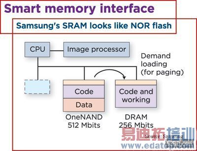
Samsung is a leaders in flash memory. With its OneNAND technology, designers can use their existing chip set’s NOR interface to communicate directly with the NAND flash memory, eliminating the need for a separate NAND device. In addition, OneNAND claims faster read/write performance than NOR flash alone.
"We think that flash has many advantages [over rotating media], such as the lower voltage. And we’re doubling our density every year," said Anu Murthy, Samsung Semiconductor’s senior strategic- marketing manager. "From a pricing point, we are able to compete with rotating [media] up to a certain density. We aren’t going to be at 60 Gbytes, for example, but we don’t see handsets heading in that direction, especially in the short term."
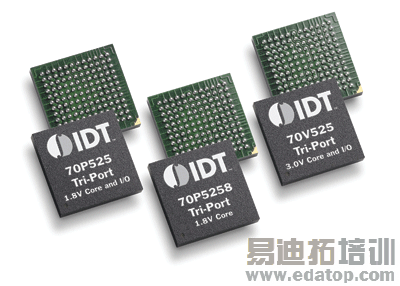
A family of Tri-Port devices from Integrated Device Technology enables simultaneous access to memory. The three- member family consists of the 70V525M and 70P525M, which have 3.0- and 1.8-V cores and I/O operation, respectively. The third part, the 70P5258M, supports 3.3-, 3.0-, 2.5- and 1.8-V I/O voltages on the three ports with a 1.8-V core. This functionality lets designers employ the three-port devices to interface with a host of current and future applications and baseband processors of differing voltages without using additional voltage translators.
上一篇:200多项专利揭示苹果触摸屏背后的秘密
下一篇:关于SIM卡不识别问题