- 易迪拓培训,专注于微波、射频、天线设计工程师的培养
高速CAN收发器的功能、特性和性能(英)
录入:edatop.com 点击:
In-vehicle networking has existed for many generations of vehicle platforms dating back more than 30 years. These days, most of the communication inside vehicles is accomplished over networks defined by established industry standards. As the number of electronic systems in new vehicles grows, so does the number of nodes that need to communicate with each other. In addition to node growth, the volume and frequency of information that needs to be shared is increasing with each new vehicle platform. Vehicle networking is evolving to include optimized buses for different tasks. Figure 1 shows some of the current and emerging standards including CAN, LIN, MOST, IEEE-1394, and FlexRay technologies.
ISO-11898 standard
Currently, controller area network (CAN), which is best suited for short, frequent communication of status and control information, is the most widely used and cost-effective networking technology for in-vehicle communications. LIN is a growing standard working as a subnetwork to CAN for tasks such as controlling the moving parts in doors and seats. Emerging FlexRay technology is poised to deliver a needed bandwidth increase for overworked networks as well as redundant and deterministic communications required for critical safety applications. The established MOST standard is aimed at audio- and video-oriented communication, while other multimedia standards are beginning to be adopted into the vehicle such as IEEE 1394 and Bluetooth.
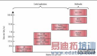 Figure 1. In-vehicle networking standards. |
The CAN standard, or ISO-11898, specifies the protocol and physical layer for two-wire differential communication and is broken into five parts. Four have been released, and Part 5 is currently in working draft status. Table 1 summarizes the five sections.
Which-or whether-ISO-11898 CAN networks are implemented varies by OEM. In general, “high speed,” as specified by Part 2 of the standard, is most often used in ignition-supplied, Clamp 15 engine networks, and “low-speed fault-tolerant CAN,” as specified by Part 3, is used in battery-supplied, Clamp 30 body networks. In new platforms, the CAN physical layer for battery-supplied nodes will be implemented either according to high speed, low power (Part 5) or as low speed fault tolerant (Part 3). Which part of the standard implemented will depend on the preference and requirements of individual OEMs.
 |
Overall, high-speed CAN is the least expensive and simplest physical layer network to implement, and is suited to power train and chassis control networks, which typically contain nodes that need to be operational only when the ignition is on. High-speed CAN allows for data rates up to 1 Mbit/sec. However, most vehicle networks communicate at 250 or 500 kbits/sec as specified in SAE-J2284. Low-speed fault tolerant CAN is more expensive to implement than high-speed but allows for continued communication in the event that one of the differential bus signal wires is inadvertently cut open or shorted to battery or ground. These networks can operate at up to 125 kbits/sec.
The new high-speed, low-power CAN is backward compatible with Part 2 of the standard and specifies features that address some limitations with Part 2 of the standard. The main addition addresses the situation in which unpowered transceivers could present low impedance to the bus and prevent powered transceivers connected to the same bus from communicating. Transceivers that are compliant with Part 5 are specified not to load the bus when unpowered. Also specified are a low-current standby mode to minimize power drain on battery-supplied nodes and a provision allowing one node to wake up other nodes remotely by asserting an extended dominant pulse onto the bus. This enables electronic functions to operate without the ignition engaged and without consuming much power from the battery while the alternator is not running.
Implementing a CAN node
There are three physical components necessary to implement a CAN node: a microprocessor, which could be a microcontroller or a DSP; a CAN hardware protocol controller; and a CAN physical layer transceiver. There are different configurations and levels of integration in which these blocks are physically implemented. When CAN technology was first introduced, nodes were implemented with three separate ICs, including a basic microcontroller, a stand-alone CAN controller, and a stand-alone transceiver. These days, one or more CAN controllers are commonly integrated into either a microcontroller or DSP, and the transceiver may be stand-alone or part of an ASIC or system-based chip, including power management, diagnostic, and other analog or digital features depending on integration costs and the functional requirements of the node.
Transceiver operation and features
The functionality of a CAN transceiver is fairly straightforward. Figure 2 shows the functional block diagram of a basic transceiver as specified by ISO-11898-2 in the common eight-pin configuration. High-speed CAN transceivers generally consist of a single-ended-to-differential driver, a differential receiver, one or more enable functions, and a VCC/2 reference.
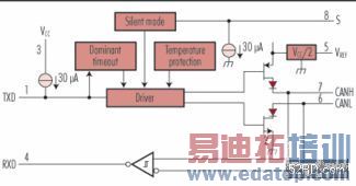 Figure 2. Functional block diagram of a sample ISO-11898-2 CAN transceiver. |
When the transceiver is driving the bus, the TXD pin senses a single-ended logic signal from the CAN controller, interprets it as either dominant, logic 0 or recessive, logic 1, and delivers an inverted, differential signal to a multinode bus terminated with 120 Ω at each end. This differential signal is defined as VOD = VCANH - VCANL and is typically 2 V for a dominant input, and very near 0 V for a recessive input with a 60-Ω typical load condition. Figure 3 illustrates the description of dominant and recessive driver behavior.
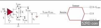 Figure 3. CAN driver functionality. |
Unlike most differential drivers, a CAN driver is designed to provide either a positive differential voltage or high impedance to the bus. This behavior is necessary because the CAN protocol incorporates a form of lossless arbitration or Carrier Sense, Multiple Access/Collision Detection + Collision Resolution (CSMA/CD+CR). It’s a pretty lengthy acronym, but the general idea is that any node can request access to the bus after an idle period. In the event that two nodes try to send a message at the same time, the node sending the most important message will be recognized and allowed to continue transmitting its message without having to restart or losing any of the bits it has already sent. The dominant/recessive behavior of the physical layer is the key to enabling this type of lossless arbitration. At the bit level, a node sending a recessive bit (one whose driver is high impedance) is able to simultaneously detect through the CAN receiver a dominant bit being sent by another node and immediately recognize that its message is a lower priority and stop transmitting. If the recessive state was driven as a negative VOD signal rather than high impedance, contention would result between a node driving dominant and another driving recessive and this type of arbitration would not be possible.
Functionally, the CAN receiver simply detects whether the voltage difference between the CANH pin and the CANL pin is greater than 900 mV or less than 500 mV and respectively provides a single-ended dominant, logic 0 or recessive, logic 1 signal to the CAN controller via the RXD pin. CAN receivers also incorporate hysteresis for noise immunity.
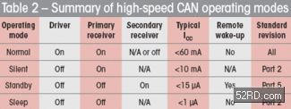
High-speed CAN transceivers are often distinguished from one another by whether a low-power mode is implemented and how it behaves. All transceivers have a normal operating mode in which the driver and a primary receiver are enabled, allowing the transceiver to transmit and receive CAN messages at normal bit rates. Normal mode requires the highest supply current. During dominant transmission, a 5-V supplied transceiver will draw about 60 mA, including load current; a 3-V supplied transceiver will draw about 40 mA. In general, a 3-V supplied transceiver will generally consume about one-half the power of a 5-V supplied transceiver in normal mode.
In addition to a normal mode, a typical high-speed CAN transceiver will also feature one or two low-power modes. The first, often referred to as “silent” or “listen” mode, occurs when the driver is disabled and the receiver is enabled. This mode prevents a node from transmitting to the bus but allows it to receive and monitor messages sent by other nodes. Silent mode can also be invoked to protect the bus if there is a fault condition, such as the CAN controller output is “stuck dominant,” and therefore would block valid communication on the bus. In silent mode, the supply current is typically about 6 mA. The second low-power mode that can be found on basic high-speed transceivers is sometimes referred to as sleep mode. In this mode, both the driver and receiver are disabled and no communication to or from the bus is desired or possible. Supply current in this mode can be held to levels less than 1 μA.
Before discussing a third low-power mode, it’s appropriate to introduce the functional block diagram of an ISO-11898-5 transceiver as shown in Figure 4.
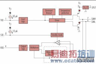 Figure 4. Functional block diagram of a sample ISO-11898-5 CAN transceiver. |
The transceivers shown in Figure 2 and Figure 4 differ in several ways. The first and most obvious is that the high-speed, low-power transceiver shown in Figure 4 has an additional receiver connected to the bus pins. This allows for the third low-power mode alluded to previously and is commonly referred to as standby mode. In this mode, the driver is disabled, the primary receiver is disabled, and a secondary low-power receiver is enabled. This secondary receiver consumes less than 15 μA of supply current and monitors the bus for a remote wake-up signal sent by another node. The remote wake-up is defined as a dominant signal with a duration between 500 nsec and 5 μsec. If the secondary receiver detects this extended dominant input, it will pass it on to the controller as an indication that another node is requesting a wake-up. The minimum pulsewidth of 500 nsec ensures that unintended dominant noise pulses will not be interpreted as valid wake-up requests. Table 2 summarizes the previous discussion on normal and low-power operating modes.
Aside from basic operation, low-power modes, and remote wake-up capability, there are some additional features worth mentioning that are common to high-speed CAN transceivers. The first is a fault protection feature known as “dominant timeout.” Several transceivers on the market have this feature built into them and some OEMs are beginning to require it. This feature prevents the driver from blocking network communications in the event of a hardware or software failure, resulting in a permanent dominant signal being fed to the driver input (TXD). This is a similar concept to the case of the silent mode turning off the driver but is implemented with a monitor circuit that is integrated into the driver input of the transceiver, as indicated in Figure 3. A timer circuit monitors TXD and is triggered by a falling edge. Once triggered, it looks for a rising edge. If no rising edge is detected within the timeout constant, typically around 500 μsec, the CAN driver will be disabled, releasing the bus of a stuck dominant signal and allowing other nodes to resume communications. It’s important to be aware and account for the dominant timeout feature when evaluating or troubleshooting recessive DC behavior on transceivers that have this feature.
 |
The final discussion concerning standard transceiver functions has to do with pin five of a standard eight-pin transceiver. This pin typically implements one of three optional functions depending on the specific transceiver. The first and simplest is to assign this pin as a second enable input to allow additional low-power modes such as those described previously. It can also be assigned as a weak VCC/2 reference, commonly called VREF, which may be used as a reference for a differential comparator that monitors the CAN receiver output. Today, the VREF pin is not commonly implemented in new automotive networks. A third function, specified as an option in the ISO-11898-5 working draft, is known as SPLIT. Like VREF, in normal mode the SPLIT pin behaves as a weak VCC/2 reference and can be connected to the center point of a node with split (common mode) termination in order to provide some stability to the common mode output. This can translate to a slight improvement in emissions performance. When the transceiver is put into standby mode, the SPLIT pin will transition to high impedance, while CANH and CANL are pulled to ground through high impedance so that the bus levels of a network in standby mode can be controlled without external supplies or other networks.
Design considerations
The most critical concern in implementing data communication networks in vehicles is electromagnetic compatibility (EMC). This is a lengthy topic, but will be mentioned briefly here because it is such an important consideration in the design and performance of CAN physical layer devices.
In general, EMC can be broken into two categories. The first is emissions and the second immunity. Emissions can be described as how electrically noisy and potentially disturbing a component is to its surrounding environment. Conversely, immunity can be thought of as how tough or robust a component is to noise from other sources. Ideally, transceivers need to be soft-spoken and have a thick skin. EMC performance is particularly important in the case of CAN transceivers because they are often employed to send safety-critical control and status data up to 30 m across an unshielded twisted pair of wires buried in a complex vehicle wiring harness.
When designing a transceiver to minimize its contribution to emissions, it’s important to focus on the driver output. In short, radiated emissions performance can be shown to correlate with the output common mode voltage at any point along the bus. Output common mode voltage is defined as VOC = (VO(CANH) + VO(CANL))/2. An example of a VOC measurement at the component level is shown in Figure 5.
 Figure 5. Driver output common mode voltage (VOC). |
In general, any fluctuation in the VOC signal is an indication that common mode current fluctuations are present in the differential twisted pair. Therefore, radiated emissions will be present and can be detected at some distance from the bus by an antennae hooked up to a spectrum analyzer. Key to minimizing emissions contributed by the CAN driver is to design it in such a way as to ensure the current in the CANH output is always equal and opposite to the current in the CANL output under all operating, process, and load variations. Assuming a perfectly balanced board layout, connector, and transmission line, this would translate to a steady-state VOC curve with no common mode current in the twisted pair and no radiated emissions emitting from the bus. In practice, this is much easier said than done.
Careful consideration must also be taken to balance the layout and loading of the CAN output signals throughout the system in order to minimize overall emissions. In order to minimize the transceiver’s contribution to overall system emissions, first-generation transceivers typically employ driver slew rate control. This is implemented by connecting a resistor between an enable pin, typically called Rs, and ground. A larger resistance corresponds to slower driver output transitions. Adjusting this resistor allows for tuning of a system to optimize emissions performance at a given data rate. Common mode chokes are often also added near the transceiver output to help minimize emissions.
Newer-generation transceivers typically don’t employ externally controllable slew rate control, but are rather designed to better match the CANH and CANL output currents before, during, and after transitions between dominant and recessive states and back. With proper board and connector layout and balancing of the transmission media, it’s possible to achieve very low emissions using a newer generation of transceiver without the addition of a common mode choke. One termination technique that can provide significant improvement in emissions is to split the termination resistor and add capacitance to the center, or common mode point, as shown in Figure 6.
 Figure 6. Typical CAN node configuration. |
Typically, a larger capacitance leads to a flatter VOC signal and a larger benefit in reducing emissions. This adds capacitance to the node, however, and has to be traded off versus maximum node load requirements. This capacitor also provides an AC path between ground and the common mode node, which could be an issue if there is ground noise on the module. When using an ISO-11898-5 transceiver, the SPLIT pin output may also be connected to the common mode termination point to provide a small stabilization benefit as noted earlier.
In the context of this article, immunity is considered to broadly cover transceiver robustness to several different defined noise sources including bulk current injection (BCI) , direct power injection (DPI), electrostatic discharge in all its forms, automotive transient pulses according to ISO-7637, and bus pin opens and shorts to ground or VCC. Application of these stresses and required transceiver performance levels vary by industry standards as well as OEM EMC specifications. Design of a robust CAN transceiver must take into consideration continued operation under BCI and DPI stresses and survival under the remaining stresses.
Designing a transceiver to protect against all these immunity stresses while meeting functional and emissions requirements is quite a complex challenge. A short list of some of the driver design considerations includes high breakdown output structures, transient clamps, current clamps, and thermal shutdown. Receiver design considerations include wide input common mode range, balancing input impedance, and balancing input thresholds and hysteresis. External components such as back-to-back zener diodes and common mode chokes can also be used to improve robustness of the node to transient and common mode noise sources. Figure 6 shows a typical CAN node with commonly deployed external components.
The reader should have a good sense of the basic functionality and features of a high-speed CAN transceiver, as well as an understanding of the key differences between Part 2 and the in-progress version of Part 5 of the CAN physical layer specification. Some insight into transceiver design considerations in response to EMC requirements also has been conveyed.
上一篇:数字电视中的负载点稳压(英)
下一篇:控制多个 LED 的功耗及成本(英)