- 易迪拓培训,专注于微波、射频、天线设计工程师的培养
数字电视中的负载点稳压(英)
录入:edatop.com 点击:
The current generation of digital televisions presents several challenges to the power designer. Many of these sets are flat-panel designs consisting of individual modules in separate locations within the chassis. These modules may consist of tuner units, main system boards, display drivers, audio sub-systems, LCD back-light drivers and other components. Each of these sub-systems can contain sensitive analog circuits, processors, CPUs, ASICs and other diverse circuitry, each with their own unique power requirements. The AC-line voltage is converted to an intermediate bus voltage and then routed to each module within the set. This voltage is typically in the range of 12 to 15 V DC. Point-of-load regulators in each module are used to convert this intermediate bus voltage to the voltages required by the individual components.
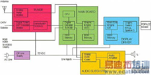
Figure 1. LCD TV Block Diagram
Consider the proposed LCD TV block diagram shown in Figure 1. Each major sub-assembly within the chassis is shown along with the key component blocks. In this example, there is a front-end tuner, main board, display driver and audio board. Each of these assemblies is supplied with 12 V from the off-line power supply. Some form of point-of-load regulation must be provided in each module to supply the required voltages for operation. Table 1 features each sub-system and the voltage and current requirements for each block, as well as any additional requirements such as sequencing or tracking.
| Sub-System | Supply Voltage (volts) | Load Current (amperes) | Sequence /Tracking | |
|---|---|---|---|---|
| Tuner | ||||
| Analog Tuner | Analog | 5.0 | 0.300 | |
| Digital Tuner | Core | 2.5 | 0.500 | Sequential |
| I/O | 3.3 | 0.300 | Sequential | |
| Demodulator | Core | 2.5 | 1.800 | Sequential |
| I/O | 3.3 | 0.300 | Sequential | |
| Main Board | ||||
| CPU | Core | 1.2 | 2.000 | Sequential |
| I/O | 3.3 | 0.600 | Sequential | |
| Vddq | 2.5 | 0.800 | Sequential | |
| Digital Decoder | Core | 1.2 | 2.000 | Sequential |
| I/O | 3.3 | 0.600 | Sequential | |
| DDR Memory | Vddq | 2.5 | 0.800 | |
| Vttq | 1.25 | 0.800 | Tracking | |
| Graphic Engine | Core | 1.2 | 2.000 | Sequential |
| I/O | 3.3 | 0.600 | Sequential | |
| Vddq | 2.5 | 0.800 | Sequential | |
| Display Driver Unit | ||||
| Back-End Engine | Core | 1.2 | 2.000 | Sequential |
| I/O | 3.3 | 0.600 | Sequential | |
| Vddq | 2.5 | 0.800 | Sequential | |
| DDR Memory | Vddq | 2.5 | ||
| Vttq | 1.25 | Tracking | ||
| Graphic Control FPGA | Core | 1.2 | 0.500 | Sequential |
| I/O | 3.3 | 1.200 | Sequential | |
| Vddq | 2.5 | 0.150 | Sequential | |
| Audio | ||||
| Stereo Audio Codec | 3.3 | |||
| Audio Amplifier | 12.0 | |||
Table 1: LCD TV subsystems with V, I and additional requirement
High-performance signal processing devices used in the main board and display driver unit, such as the FPGAs and DSPs, require multiple power supplies that generate different voltages for the core and I/O voltages. The sequence in which the supply outputs power "up" and "down" is critical to device operation and long- term reliability. There are three distinct methods of power sequencing: sequential, ratio-metric and simultaneous. The appropriate sequencing method is dependent on the processor’s requirements. For this example the sequential method is specified, where one power supply ramps up and settles to its final regulation voltage, and then the second power supply ramps up after a time delay.
Figure 2 shows an example of the sequential method. A useful method to implement this sequencing scheme is to use devices that feature integrated power good and enable functions. Connect the power good output of the first supply to the enable pin of the second supply to be sequenced. Make sure that polarity of the signals is correct. Most DC/DC converters that contain these features are meant to be used in this manner and the polarities will be consistent and the signals can be tied directly together. Additional supplies can also be controlled in this manner.
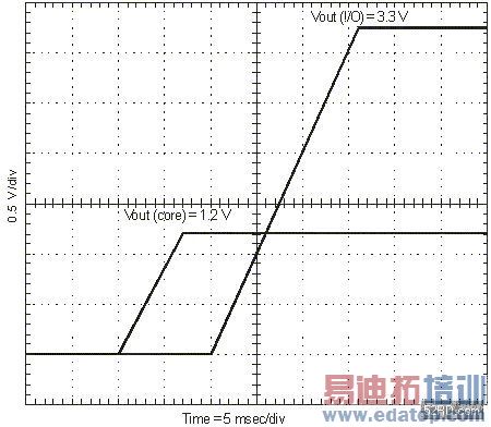
Figure 2. Sequencing Supply Waveforms
Double data rate (DDR) memory systems require both Vddq and Vtt voltage rails. While a standard supply type may be used for the Vddq output, a different type of power supply is required for the bus termination Vtt voltage. For these DDR bus termination supplies, the Vtt voltage generation circuit must be able to accurately track a reference voltage, Vref, which is 50 percent of the output supply voltage, Vddq. While Vddq may vary by +/- 200 mV from its nominal value of 2.50 V, Vtt must remain within ?0 mV of Vref under all load and transient conditions. The circuit generating Vtt must also be able to sink current when the output buffer (line driver) is at a logic-high state and source current when the output buffer state is low. With the current-sinking mode, the current through the output inductor is reversed from the normal direction in a buck configuration.
In the sinking mode, the switching process is similar to that of a boost converter, except that the current flows into the output of the power supply, gets boosted, and flows out to the input supply rail. Control circuits must function properly when both sourcing and sinking current. A specialized converter such as Texas Instruments’ TPS54372 DC/DC converter works well in these applications as it is designed for bus termination circuits with voltage-tracking requirements.
Figure 3 shows a possible power solution. For each sub-system, the power requirements are combined so that a single regulator can be used at each point of load, and only the 12 V intermediate bus voltage is distributed through the chassis.
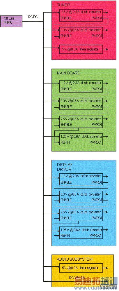
Figure 3. Power System Architecture
Conclusion
For the analog tuner, it may be desirable to use a linear regulator for the power source. Even though the efficiency will suffer, the sensitive analog stages may require the noise suppression of a linear regulator. If power dissipation is a factor, the intermediate bus can be pre-regulated to a lower voltage and a low drop-out type linear regulator can be used. For powering the processors, ASICs and FPGA digital circuitry, DC/DC converters are the best choice. They offer higher efficiencies and lower power dissipation than linear regulators and are able to supply higher currents. Using converters with additional features such as enable and integrated power good signals make sequencing core and I/O voltages much simpler, as shown in those blocks. Be sure to pay special attention to the unique requirements of bus termination voltages.