- 易迪拓培训,专注于微波、射频、天线设计工程师的培养
通过切换 ADC 的取样边来精确测量 ADC 驱动电路的建立时间(英)
录入:edatop.com 点击:
[Editor’s note to readers: this article has several corrections: Figure 3 is corrected; also, some math symbols in equations in "Averaging to Achieve Better Resolution" and in "Bias Current Calculation" sections are corrected (both are at the end of the article). We apologize for any confusion]
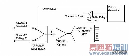
Figure 1: Evaluation setup for evaluation
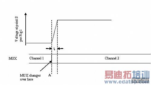
Figure 2: Behavior of MUX output with time
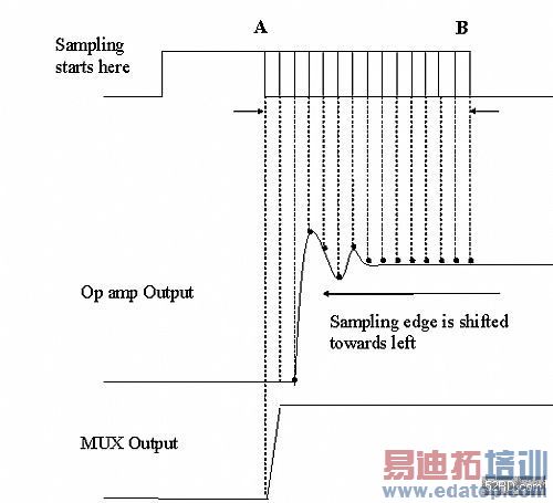
Figure 3: Sample edge shifting method

Figure 4: The equivalent circuit of ADC input when sampling switch is closed
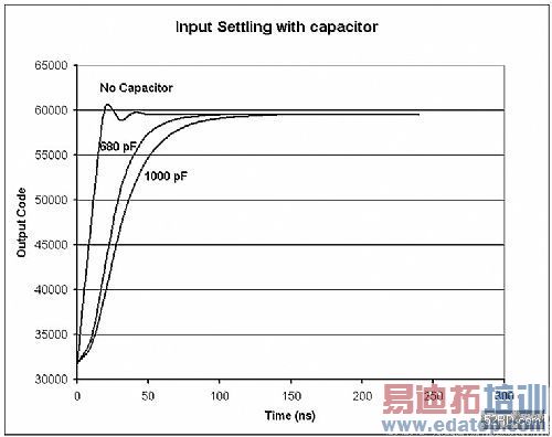
Figure 5: Input settling behavior of the ADC with different values of capacitors
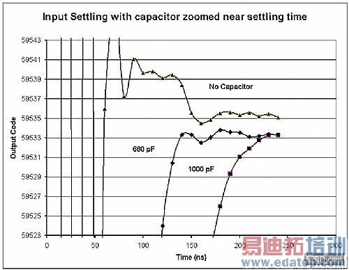
Figure 6: Input settling behavior, shown zoomed near the settling zone
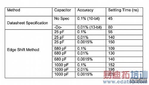
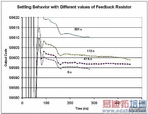
Figure 7: Input settling behavior with different values of op amp feedback resistor
The linearity and distortion performance of an analog-to-digital converter (ADC) is dependent upon the analog input settling. Thus, it is important to measure the settling time of the driving circuit including the operational amplifier (op amp), analog multiplexer, and other associated circuitry for a high resolution (more than or equal to 14-bit) high-speed ADC.
The method discussed here plots the settling behavior of an op amp which drives a high resolution ADC. It characterizes the settling time of the op amp with the ADC and op amp in the system. The accuracy of the measurement is improved beyond the ADC resolution with the help of averaging. It takes the help of the high-resolution ADC itself to plot the settling behavior, thus we can measure the settling time of the op amp with the ADC in the system.
Introduction
Many modern data acquisition systems consist of high-speed, high-resolution ADCs (Reference 1). CMOS switched-capacitor-based ADCs are often chosen for such designs, due to low cost and low power dissipation. These ADCs use an unbuffered front end directly coupled to the sampling network. To effectively drive the ADC with minimal noise and distortion of the wanted signal, it is necessary to drive the ADC with a high-speed, low-noise and low-distortion op amp (Reference 2).
To achieve minimal distortion, it is important that the op amp output settles to the desired accuracy within the acquisition time of the ADC. Normally the op amp settling time is calculated either from the frequency response specified in the op amp datasheet, or by probing the output with an oscilloscope which has a limitation on resolution. Sometimes the difference between the op amp input and output is amplified to achieve better accuracy (Reference 3). These methods are limited by oscilloscope resolution or circuit parasitics. Moreover, the settling time of the op amp is affected by the parasitic capacitance and inductance introduced by the oscilloscope probe.
In another method, the difference between the output and input is amplified to increase the resolution of the measurement. None of these methods include the parasitic capacitance and inductance present in the ADC sampling circuit and package.
Definition of Settling Time
Settling time is the time period between the application of an ideal, instantaneous step input to the time at which the closed-loop amplifier output has entered and remained within a specified error band, usually symmetrical about the final value. Settling time includes a very brief propagation delay, plus the time required for the output to slew to the vicinity of the final value, recover from the overload condition associated with slewing, and finally settle to within the specified error. For high-resolution ADCs, the specified error band is usually one-fourth of an LSB (least significant bit) of the ADC.
Basic Setup
The ADC used here is Texas Instruments ADS8411, an ADC with a 16-bit, 2 Msps successive-approximation register (SAR) architecture. The driver op amp is Texas Instruments THS4031. Figure 1 shows the evaluation setup.
Figure 1: Evaluation setup for evaluation
The instantaneous step input is generated by an analog multiplexer (Texas Instruments TS5A3159) by switching its two channels. A dc voltage, V, is applied to channel 2, and channel 1 is connected to ground. (This setup can produce a step input rising to V from 0 or falling to 0 from V. Alternatively, the step input can be generated by any step generator. The step generator should settle much faster than the op-amp settling time.
Step 1: ADC samples channel 1 (connected to ground) first. A long sampling time is provided for sampling to make sure that the input capacitor of the ADC is fully discharged.
Step 2: The analog MUX is switched to channel 2 from channel 1 at instant A in Figure 2.
Figure 2: Behavior of MUX output with time
The diagram shows the voltage at point S (Figure 1) when the MUX switches to channel 2 from channel 1. The settling time of the MUX is denoted by ts. Note that we assume that ts is much less than op amp settling time.
Step 3: Once the analog MUX is switched at instant A, the input of the op amp starts changing. The output of the op amp starts changing after a very brief propagation delay after instant A. The settling time (tideal) is approximately calculated from the slew rate and the bandwidth specified in the op amp datasheet. The proposed method plots the op amp output from instant A to instant B (Figure 3).
Figure 3: Sample edge shifting method
The time difference between instant B and instant A is two times tideal.
Step 4: First ADC sampling edge appears at instant B and n number of readings (digital outputs from the ADC) are taken. Average is taken on n number of readings for better accuracy of the result (See next section).
Next, the sampling edge is shifted by 1 ns (with the help of pattern generator and adjustable delay generator of Figure 1) to the left (Figure 3) and, again, n number of readings are taken. This way the sampling edge is shifted towards left from instant B to instant A with a step of 1 ns. At each sampling edge, the average is stored in an element of an array. The array is plotted against the time to get the true picture of the op amp output settling (Figure 3).
Averaging to Achieve Better Resolution
The input of an N-bit ADC should settle to at least N+2 bits. But the measured output is an N-bit digital code from the ADC.The resolution can be increased by repeatedly sampling the same input and taking multiple (n) readings from the ADC. Finally, an average is taken on n digital output codes. It can be shown that for each additional bit of resolution, the number of readings should be increased by a factor of 4. Therefore, "w" extra bits of resolution requires 4wreadings.
For each additional bit, the signal-to-noise ratio (SNR) increases by 6.02 dB. In this case, the 16-bit ADC should settle at least to 18-bit accuracy.
SNR = 6.02 x N + 1.76
Where N = resolution of the ADC.
SNR = 110.12 dB for 18-bit performance
Extra bit (w) of resolution required
= (110.12 - 86*)/6.02 ≈4
(where * is the typical SNR specification of the ADS8411)
Number of samples (n) needed for each reading
= 44 = 256
Results
An RC filter is used at the output of the op amp to filter the external noise. The ADC sampling circuit always consists of another RC (here, R’ and C’) shown in the Figure 4.
Figure 4: The equivalent circuit of ADC input when sampling switch is closed
Figure 5 shows the settling behavior with three different values of external capacitors (C in figure) used for RC filtering.
Figure 5: Input settling behavior of the ADC with different values of capacitors
Figure 6 is a zoomed version of Figure 5, to show the settling more accurately.
Figure 6: Input settling behavior, shown zoomed near the settling zone
One code signifies one LSB at 16-bit resolution. The resolution of the measurement is more than 16-bits, because 65,536 samples were captured and averaged for each reading. The result shows significant ringing when there was no capacitor. This also reveals the fact that the system was under-damped when no capacitor was used. Also note that use of a bigger capacitor (1000 pF) significantly increases the settling time.
The Table shows a comparison of result with this method versus traditional method: Here, R = 20 Ω; 0.0015% implies one LSB in 16-bits
By averaging the output data the resolution of the result can be improved beyond 16-bits.
Measurement of Bias Current
Figure 7 shows op amp settling behavior with different values of feedback resistors.
Figure 7: Input settling behavior with different values of op amp feedback resistor
The difference in the settled voltage indicates the offset voltage because of bias current. From this the calculated bias current is 3 μA which matches with the typical specification of THS4031. This experiment validates the correctness of this setup.
Bias Current Calculation
The settled value (with 0 Ω in the feedback)
= 59595 (digital code)
The settled value (with 301 Ω in the feedback)
= 59610 (digital code)
Delta (Offset Voltage)
= bias current x resistor (used in the feedback)
Delta (Offset Voltage)
= (59610 - 59595) x (4.096V)/65536 = 938 μV
Bias Current = 938 μV/301 Ω = 3.12 μA
(compared to datasheet typical specification of 3 μA)
Conclusion
This is a practical and simple method to accurately measure the settling time of ADC driving circuit. The settling behavior is unaffected by the measurement, because no additional component is used for the setup. This method can be implemented as a Built-in-Self-Test (BIST) in future. The averaging of multiple reading improves the accuracy of the result.
上一篇:数字控制测量系统内响应(英)
下一篇:分析与测量运算放大器电路中的固有噪声 – 第 2 部分:运算放大器噪声简介(英)