- 易迪拓培训,专注于微波、射频、天线设计工程师的培养
CST2013: Bend Sheet or Thin Shape
录入:edatop.com 点击:
 Modeling: Tools
  Bend Shape
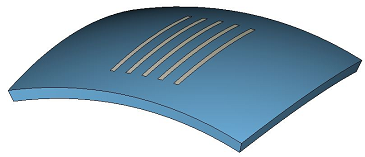
This operation allows to wrap one or more thin planar sheets or shapes around a solid. Sheets can be created by covering a planar curve or by creating a brick with zero height.
You may bend on solids that consist of a developable surface (e.g. planar, cylindrical, conical, or spline surfaces) or on solids that consist of a not developable surface (e.g. spherical, toroidal surfaces or faces created by sweeping a spline curve along a non-linear path).
Note that when bending on solids with not developable surfaces then it is not assured that the edge lengths are preserved.
First select the sheets or thin shapes you want to bend and then follow the steps on the screen.
| Bend Shape |
|
Please note: For multiple selected sheets or shapes it is necessary that all sheets or shapes lie in the same plane, and at least one sheet or shape lies on the surface of the solid.
Examples
Bend sheet on cylinder or cone
Bend sheet on sphere
Bend sheet on a solid that consists of a not developable surface
Bend a printed-circuit board (PCB) design with thick layers on a solid
Example of the workflow
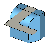
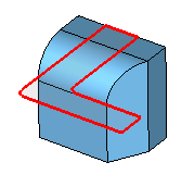
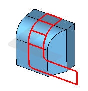
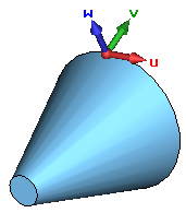
1. Step: Select sheet to bend
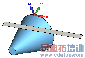
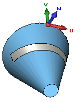
| 2. Step: Select solid to bend on | 3. Step: Select face to bend on |
|
|
|
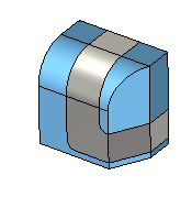
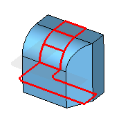
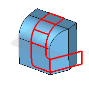
4. Step: Select the next face to bend on | 5. Step: Select the next face to bend on | 6. Step: Finish the bending operation by pressing RETURN |
|
|
|
Example: Bend sheet on cylinder or cone
For bending a sheet on a cylinder or a cone, it is important to align the sheet correctly on the cylindrical or conical shell.
Note that the bending might not work if the sheet intersects the solid.
To ensure that the sheet is placed correctly on the solid, follow the next steps.
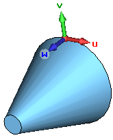
1. Step: Align the local wcs on a point on the solid | 2. Step: Pick the cylindrical or conical surface | 3. Step: Align wcs on the picked face |
|
|
|
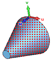
4. Step: Create or align your sheet in the u-v-plane | 5. Step: Bend the sheet on the solid as explained in the previous example | |
| | |
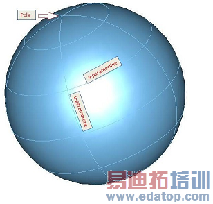
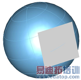
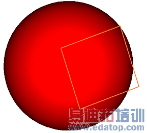
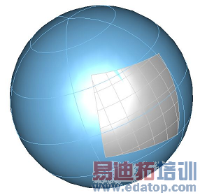
Example: Bend sheet on sphere
When bending a sheet on a sphere then the sheet is bent on the parameter space of the sphere. Spheres are singular in u at the poles. Therefore bending is not possible when the projection of the sheet lies on the pole of the spherical face.
To display the poles of the sphere, you may use View View Options Specials ( ) and check Draw surface mesh.
The next steps show the bending of a sheet on a sphere:
1. Step: Align the sheet on the sphere | 2. Step: Pick the spherical surface | 3. Step: Bend the sheet on the sphere |
|
|
|
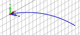
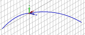
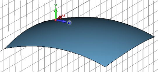
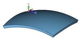
Example: Bend sheet on a solid that consists of a not developable surface
For creating a solid with a not-developable or doubly-curved surface, we are sweeping a spline curve along a non-planar path.
1. Step: Create a spline curve, and align local wcs on an endpoint of the curve and rotate it 90 degree by v-axis | 2. Step: Create a new spline curve by starting in the origin of the local wcs | 3. Step: Sweep first curve along second curve (each curve item has to be in its own curve component) |
|
|
|
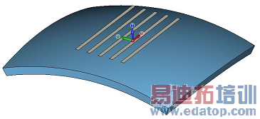
4. Step: By thickening the selected face you get a solid with a doubly-curved surface | 5. Step: To create your sheet(s) which you want to bend, first align local wcs with a point on the face, and then with the face of the solid. | 6. Step: Now bend the sheet(s) on the solid as explained in the firsts example
|
| |
|
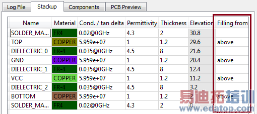
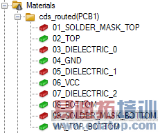
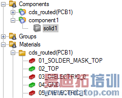
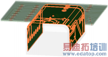
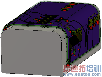
Example: Bend a printed-circuit board (PCB) design with thick layers on a solid
For bending a PCB please note the following:
Layers which have the same bottom coordinate should be bent together.
Vias must be bent together with the bottom or top layer.
Multiple selection of material layers is possible and very useful for the selection.
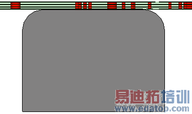
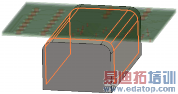
1. Step: Import your PCB data. In the EDA import dialog, for all layers use the setting "above" for the "Filling from" option. | 2. Step: Create the solid on which you want to bend the PCB. Position the solid such that one planar face of the solid touches the bottom of the layer stackup. | |
|
| |
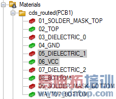
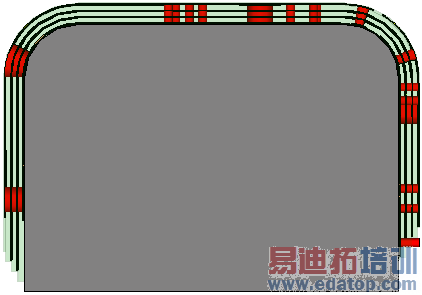
3. Step: Select the layer which is touching the top face of the brick.
| 4. Step: Start the bending operation and select the brick by double-clicking in the 3d view. | 5. Step: Select the faces on which you want to bend the PCB layer, and confirm the bending by pressing RETURN. |
|
|
|
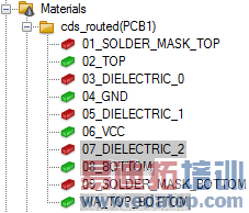
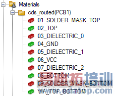
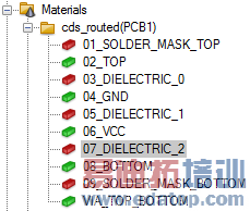
6. Step: Select the next layers which have the same bottom coordinate and are touching the already bent solder mask layer. | 7. Step: Select the already bent solder mask layer. | 8. Step: Select the faces on which you want to bend, and confirm the bending by pressing RETURN. |
|
|
|
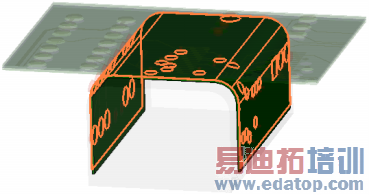
9. Step: Select the next layers which have the same bottom coordinate and are touching the already bent dielectric layer. | 10. Step: Select the already bent dielectric layer. | 11. Step: Select the faces on which you want to bend, and confirm the bending by pressing RETURN. |
|
|
|
12. Step: Now you may continue in the same way to bend the remaining layers of the PCB. | ||
|
| |
CST微波工作室培训课程套装,专家讲解,视频教学,帮助您快速学习掌握CST设计应用
上一篇:CST2013: Create a Cone
下一篇:CST2013: Import Mentor Graphics Hyperlynx Files
CST培训课程推荐详情>>
 最全面、最专业的CST微波工作室视频培训课程,可以帮助您从零开始,全面系统学习CST的设计应用【More..】
频道总排行
- CST2013: Mesh Problem Handling
- CST2013: Field Source Overview
- CST2013: Discrete Port Overview
- CST2013: Sources and Boundary C
- CST2013: Multipin Port Overview
- CST2013: Farfield Overview
- CST2013: Waveguide Port
- CST2013: Frequency Domain Solver
- CST2013: Import ODB++ Files
- CST2013: Settings for Floquet B