- 易迪拓培训,专注于微波、射频、天线设计工程师的培养
高灵活性的上转换架构符合全球无线标准(英)
录入:edatop.com 点击:
Achieving the goal of seamless voice and data connectivity affects the design requirements for wireless infrastructure. System capacity must increase. This requires larger bandwidth signals and multi-carrier capabilities. Higher power transmitters and more sensitive receivers extend the coverage range. To ensure ubiquitous coverage, the network needs smaller pico base stations to provide service to every nook of the city. Original equipment manufactures (OEMs) must be able to supply equipment that delivers this improved performance while maintaining efficient design practices and managing design costs. 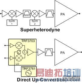
1. Superheterodyne and Direct Up-conversion Architectures. 
Additionally, OEMs must employ systems that work in a variety of existing wireless standards including CDMA2K, WCDMA, GSM and EDGE, as well as emerging standards such as TD-SCDMA employed in China and WiMAX for broadband data services worldwide. A flexible architecture that works in most or all of these types of modulation cases serves well for minimizing design resources and improving reliability. Complexity is increased because frequency bands of operation vary globally. Frequencies from 800MHz to 2.1GHz are used for most voice communications, with the 3.5-GHz and 5.6-GHz ranges addressing data services.
These variables require a flexible up-converter with the RF performance to meet stringent base station specifications, all while maintaining good integration for a cost-effective and compact design. It must be capable of serving the multitude of frequency bands and a variety of the wireless modulation standards.
Transmitter Architecture
The two major architecture options for the transmitter are direct upconversion and superheterodyne. The traditional superheterodyne architecture consists of two mixing stages where the signal is first up-converted to a fixed intermediate frequency (IF) and then passed through a narrow band surface acoustic wave (SAW) filter. The direct conversion approach bypasses the IF stage and converts the signal directly from base band to the RF channel of choice. The block diagram of both architectures is shown in Figure 1.
The direct upconversion approach utilizes a quadrature modulator and eliminates an additional mixing stage, an additional synthesizer, and a SAW filter. This greatly simplifies the design and reduces the bill of material (BOM) costs. This approach also offers the greatest flexibility, as it can be used for a variety of modulation schemes including CDMA, GSM, and OFDM.
Since there is no narrow band filter, the architecture can support a variety of signal bandwidths commensurate with the modulation scheme of choice. For example, the various bandwidths associated with CDMA2K and WCDMA can be supported as well as the variety of WiMAX signal bandwidths that typically range from 3.5 to 10MHz. Multi-carrier applications are equally supported since there is no bandwidth restriction.
Additionally, the direct upconversion architecture sustains digital predistortion linearization (DPD) signals which must be up to five times the bandwidth of the desired signals to incorporate the third and fifth order products that are tailored to cancel out the nonlinear effects of the power amplifier.
Direct Up-Convert Modulator
The direct upconversion modulator consists of differential in-phase (I) and quadrature-phase (Q) signals that are summed together at the output. It is imperative to use the quadrature modulator for the direct upconversion approach because the local oscillator (LO) component and the unwanted image signal, or sideband, are naturally suppressed without the need for a filter.
The amount of sideband suppression is determined by the amplitude and phase balance of the input quadrature components. The LO feedthrough is determined by the DC offset balance between the two input paths. It is best to have a device that inherently provides better than 35dB of suppression on each of these parameters as there is likely degradation over temperature. If further suppression is required, additional fine-tuning can be accomplished in the digital-to-analog converter (DAC). (It is best if the data converter supplies the I/Q interface with built-in adjustment capabilities for amplitude and phase balance as well as DC offset correction.)
The key RF parameters for the modulator include output power at 1-dB compression (P1dB), output third-order intercept point (OIP3), carrier feedthrough, sideband suppression, and output noise. The linearity and output noise parameters of the modulator are critical parameters that set the system performance because they dictate the operating output range of the device and limit the maximum output power of the entire radio. Good values for these specifications would be +9dBm P1dB and -163 dBm/Hz output noise. For high peak-to-average ratio (PAR) signals like CDMA and OFDM, the modulator must pass the peaks of the signal without significantly degrading the adjacent channel power ratio (ACPR) performance that is critical to maintaining compliance to the standard.
ACPR performance can theoretically be improved by simply backing off the output power. If the device adheres to the standard model, the third order products should decrease 3dB for every 1dB of signal back-off. At some point, the noise floor of the device, which is unchanging, will dominate the ACPR performance. The key is to operate the modulator at a high enough level such that the ACPR performance is not limited by the noise floor of the device, but not too high such that it is degraded by the linearity of the device. That optimum level is dependant on the PAR of the modulation signal and the number of carriers. In most cases the optimal window is only 1 or 2-dB wide.
The noise floor performance also dictates the spurious compliance of the radio for a given output power. For example, the output power from the modulator is set to -10dBm to provide sufficient linearity. A 20-W radio would require an additional 53dB of gain from the modulator output to the antenna input. Assuming no noise filtering and no additional noise contribution from subsequent stages, the output noise level in a 1-MHz bandwidth (a typical noise bandwidth specification found in the standards) is calculated by:
Noise Power+ 1 MHz BW [dB] + Gain= Noise Power Out
-163 dBm/Hz + 60 dB-Hz+53 dB = -50 dBm
This configuration would satisfy spurious output performance of -50dBm per 1-MHz bandwidth across all frequencies.
Synthesizer
The modulator requires a synthesized local oscillator (LO) source that can be programmed to the output channel of choice. The traditional method of implementing this synthesizer uses a phase-locked-loop (PLL) chip with an external voltage-controlled oscillator (VCO). Though this approach provides good performance, the VCO device is typically large, costly, and operates over a narrow band of frequencies. Implementing an integrated synthesizer greatly reduces the circuit complexity. The integrated synthesizer only requires an external loop filter because the VCO is integrated on the silicon. The loop filter can be optimized for fast lock times typically required in TDD systems. This type of device could also incorporate a divide-by-two and divide-by-four feature that allows one device a much broader range of operation.
Though an integrated synthesizer reduces size and cost, the phase noise performance is a key parameter that cannot degrade. The phase noise of the LO will be transferred to the output signal of the modulator. For wide bandwidth signals related to CDMA, this is not as critical as for narrower band signals like GSM, and for high sub-carrier systems like OFDM modulation used in WiMAX signals. The phase noise of the synthesizer definitely impacts the Error Vector Magnitude (EVM) performance of the transmitter. A good specification here would be in the neighborhood of -160dBc/Hz at 10 MHz offset closed loop phase noise at 1.8GHz. Improvements are possible with devices optimized for lower frequencies.
Measurement Results
The transmitter direct upconversion architecture is used in the TSW3003 reference design from TI. The board incorporates a DAC5687 device which drives the TRF3703 quadrature modulator. The LO source is provided by the TRF3761 integrated synthesizer. The ACPR performance of the board with a WCDMA signal is shown in Figure 2. The performance illustrates a single carrier output power of -12dBm with an ACPR performance of -77dBc at 2.17GHz.
2. ACPR performance of the TI TSW3003 reference design with a WCDMA signal.
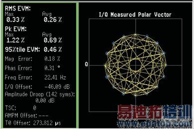
For EDGE signals, it is important to evaluate the EVM. Figure 3 shows the EVM performance for the TSW3003 board. Measurement results at 1800MHz demonstrate EVM performance of less than 0.5%.
3. EVM performance of the TI TSW3003 reference design with an EDGE signal.
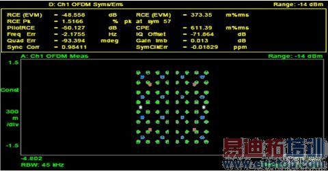
EVM is also a critical parameter for WiMAX signals that use 64-QAM OFDM modulation. For WIMAX applications, the upconversion architecture should achieve better than -40 dB EVM at 2.5-GHz output (Figure 4). This allows sufficient margin for the unavoidable degradation in the power amplifier.
4. EVM performance of the TI TSW3003 reference design with a WiMAX signal.
When selecting an up-conversion architecture, it is important to ensure that the device satisfies the key RF performance parameters for the application. A flexible architecture can help OEM designers reduce cost and size without sacrificing performance or compliance to particular regulatory specs.