不对称带状线特性阻抗计算器
录入:edatop.com 点击:
Asymmetric Stripline Impedance Calculator
Inputs
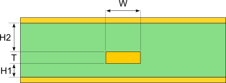
Trace Thickness
T
Substrate Height
H1
Substrate Height
H2
Trace Width
W
Substrate Dielectric
Er
Outputs
Impedance (Z):
Introduction
The asymmetric stripline transmission line is most commonly found in a pcb where the distance from trace to planes is not the same distance above and below. The ability to model this impedance is nice because it can often be found in designs. Modeling approximation can be used to design the asymmetric stripline trace. By understanding the asymmetric stripline transmission line, designers can properly build these structures to meet their needs.
Description
A stripline is constructed with a flat conductor suspended between two ground planes. The conductor and ground planes are separated by a dielectric. The distance between the conductor and the planes is not the same for both reference planes. This structure will most likely be manufactured with the printed circuit board process.
Example
An example of an asymmetric stripline is a 4 layer pcb were a trace on layer 3 is referenced to both layer 1 and layer 4. The trace is closest to layer 4 and layer 4 has the dominant effect on the transmission line impedance, but layer 1 would still affect the characteristic impedance of this trace.
Asymmetric Stripline Transmission Line Models
Models have been created to approximate the characteristics of the microstrip transmission line. The source for these formulas are found in the IPC-2141A (2004) “Design Guide for High-Speed Controlled Impedance Circuit Boards”.
上一篇:带状线特征阻抗计算器
下一篇:耦合带状线特征阻抗计算器
易迪拓培训课程列表详情>>
我们是来自于研发一线的资深工程师,专注并致力于射频、微波和天线设计工程师的培养